
Light-emitting diode epitaxial structure with pn-doped quantum barrier and preparation method thereof

A technology of light-emitting diodes and quantum barriers, applied in semiconductor devices, electrical components, circuits, etc., can solve the problems of InGaN quantum well band tilt, low internal quantum efficiency, and large GaN lattice mismatch, so as to increase internal quantum efficiency , reduce the electric field strength, increase the effect of overlapping probability

Active Publication Date: 2020-02-18
SOUTH CHINA UNIV OF TECH
View PDF4 Cites 0 Cited by
  • Summary
  • Abstract
  • Description
  • Claims
  • Application Information

AI Technical Summary

Problems solved by technology

[0007] The present invention aims at the problems of low internal quantum efficiency caused by the large mismatch between the InGaN well and the GaN lattice of the existing GaN-based light-emitting diode epitaxial wafer, the energy band of the InGaN quantum well is inclined, and the serious separation of electron-hole wave functions, and proposes a method with Light-emitting diode structure and preparation method of PN double-doped quantum barrier

Method used


Image

  • Light-emitting diode epitaxial structure with pn-doped quantum barrier and preparation method thereof
  • Light-emitting diode epitaxial structure with pn-doped quantum barrier and preparation method thereof
  • Light-emitting diode epitaxial structure with pn-doped quantum barrier and preparation method thereof

Examples


Embodiment Construction

[0039] The present invention will be further described below in conjunction with the accompanying drawings and embodiments, but is not limited thereto.

[0040] The following is only as an example, a light emitting diode epitaxial structure with PN doped quantum barriers

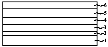
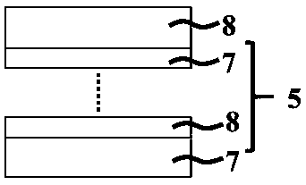
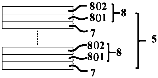
[0041] like figure 1As shown, the light-emitting diode is sequentially composed of sapphire substrate 1, GaN nucleation layer 2, unintentionally doped GaN layer 3, N-type GaN conductive layer 4, multi-quantum well active region 5 and P-type InGaN from bottom to top. conductive layer6. From bottom to top, it includes sapphire substrate, GaN buffer layer, N-type GaN conductive layer, multi-quantum well active region and P-type GaN conductive layer. The quantum well layers and quantum barrier layers in the multi-quantum well active region can be arranged alternately periodically (The order is adjustable); the quantum barrier layer is composed of a P-type doped quantum barrier and an N-type doped quantum barri...


PUM

PropertyMeasurementUnit
thicknessaaaaaaaaaa
thicknessaaaaaaaaaa
thicknessaaaaaaaaaa

Abstract

The invention discloses an LED epitaxial structure with a PN doped quantum barrier and a preparation method of the LED epitaxial structure. The LED structure comprises a sapphire substrate, a GaN buffer layer, an N type GaN conducting layer, a multi-quantum well active region and a P type GaN conducting layer from bottom to top; and the LED structure is characterized in that the quantum well active region comprises a quantum well layer and a quantum barrier layer, and the quantum barrier layer is composed of a P type doped quantum barrier and an N type doped quantum barrier. According to the invention, a micro PN junction quantum barrier replaces a traditional quantum barrier, a polarized electric field of the quantum well can be shielded, wave function separation of an electron cavity is reduced, and the light emitting efficiency of an LED is improved.

Description

technical field [0001] The invention relates to the technical field of light-emitting diodes, in particular to a light-emitting diode epitaxial structure with PN-doped quantum barriers and a preparation method thereof. Background technique [0002] Light-emitting diode (referred to as "LED") is a semiconductor solid-state light-emitting device, which uses the conduction band electrons and valence band holes inside the semiconductor material to undergo radiative recombination, and releases energy in the form of photons to directly emit light. By designing different bandgap widths of semiconductor materials, light-emitting diodes can emit light in different bands from infrared to ultraviolet. [0003] Nitride light-emitting diodes have been widely developed around the world due to their advantages of high efficiency, energy saving, long life and small size. Ultraviolet light-emitting diodes with a light emission wavelength of 210-365nm have broad application prospects in the ...

Claims


Application Information

Patent Timeline
Patent Type & Authority Patents(China)
IPC IPC(8): H01L33/06H01L33/00H01L33/32
CPCH01L33/007H01L33/06H01L33/32
Inventor 徐明升周泉斌王洪
Owner SOUTH CHINA UNIV OF TECH
Learn More