LED epitaxial wafer grown on Si substrate through L-MBE and MOCVD technologies, and preparation method for LED epitaxial wafer
A technology for LED epitaxial wafers and substrates, applied in electrical components, circuits, semiconductor devices, etc., can solve the problems of low Al atom mobility, large tensile stress of epitaxial layer, cracking of epitaxial layer, etc., and achieve excellent electrical and optical properties , Excellent crystal quality, high crystal quality effect
- Summary
- Abstract
- Description
- Claims
- Application Information
AI Technical Summary
Problems solved by technology
Method used
Image
Examples
Embodiment 1
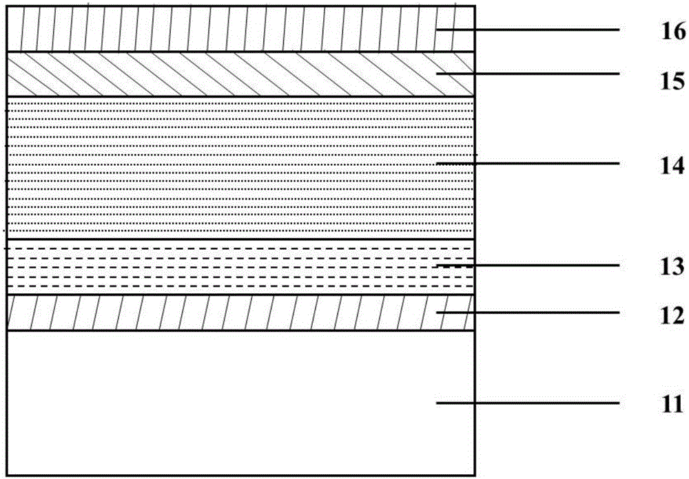
[0028] Such as figure 1As shown, an LED epitaxial wafer grown on a Si substrate by L-MBE and MOCVD technology, including a Si substrate 10 and a single crystal Al thin film 12, an AlGaN buffer layer 13, n -GaN layer 14, InGaN / GaNMQWs quantum well layer 15 and p-GaN layer 16; from single crystal Al thin film 12 to the direction of n-GaN layer 14, the content of Al component in AlGaN buffer layer 13 reduces gradually; Said single The crystal Al thin film 12 is grown by L-MBE method, and the AlGaN buffer layer 13, n-GaN layer 14, InGaN / GaN MQWs quantum well layer 15 and p-GaN layer 16 are grown by MOCVD method.
[0029] A preferred solution is that the content of the Al component in the AlGaN buffer layer gradually decreases from 70%-75% to 10%-20% from the single crystal Al thin film to the direction of the n-GaN layer.
[0030] The preferred scheme is that the thickness of the single crystal Al thin film is 20-50nm; the thickness of the AlGaN buffer layer is 200-1000nm; the th...
Embodiment 2
[0041] This example is improved on the basis of Example 1. The difference from Example 1 is that before being transferred to the MOCVD reaction chamber, the single crystal Al thin film is placed in an annealing furnace and heated at 800°C under nitrogen Annealing is carried out under the atmosphere; then it is taken out and then transferred to the MOCVD reaction chamber for the next epitaxial growth, and the subsequent growth process is the same as that in Example 1.
PUM
| Property | Measurement | Unit |
|---|---|---|
| Thickness | aaaaa | aaaaa |
| Thickness | aaaaa | aaaaa |
| Thickness | aaaaa | aaaaa |
Abstract
Description
Claims
Application Information
 - R&D
- Intellectual Property
- Life Sciences
- Materials
- Tech Scout
- Unparalleled Data Quality
- Higher Quality Content
- 60% Fewer Hallucinations
Browse by: Latest US Patents, China's latest patents, Technical Efficacy Thesaurus, Application Domain, Technology Topic, Popular Technical Reports.
© 2025 PatSnap. All rights reserved.Legal|Privacy policy|Modern Slavery Act Transparency Statement|Sitemap|About US| Contact US: help@patsnap.com


