Preparation method of self-aligned contact hole

A self-aligned contact hole and self-aligned contact technology, which is applied in semiconductor/solid-state device manufacturing, semiconductor/solid-state device testing/measurement, electrical components, etc., can solve problems such as high cost and difficult polymer monitoring and control , to achieve the effect of ensuring uniformity, good removal uniformity, and avoiding excessive polymer residue

Active Publication Date: 2019-06-28
SHANGHAI HUAHONG GRACE SEMICON MFG CORP
View PDF9 Cites 0 Cited by
  • Summary
  • Abstract
  • Description
  • Claims
  • Application Information

AI Technical Summary

Problems solved by technology

This method is difficult to realize the monitoring and control of the polymer in the process of etching, photoresist ashing and wet cleaning of the self-aligned contact hole process, even if the existing self-aligned contact can be realized. Polymer membrane monitoring and control at various stages of the pore process, also very costly

Method used


Image

  • Preparation method of self-aligned contact hole
  • Preparation method of self-aligned contact hole
  • Preparation method of self-aligned contact hole

Examples


Embodiment 1

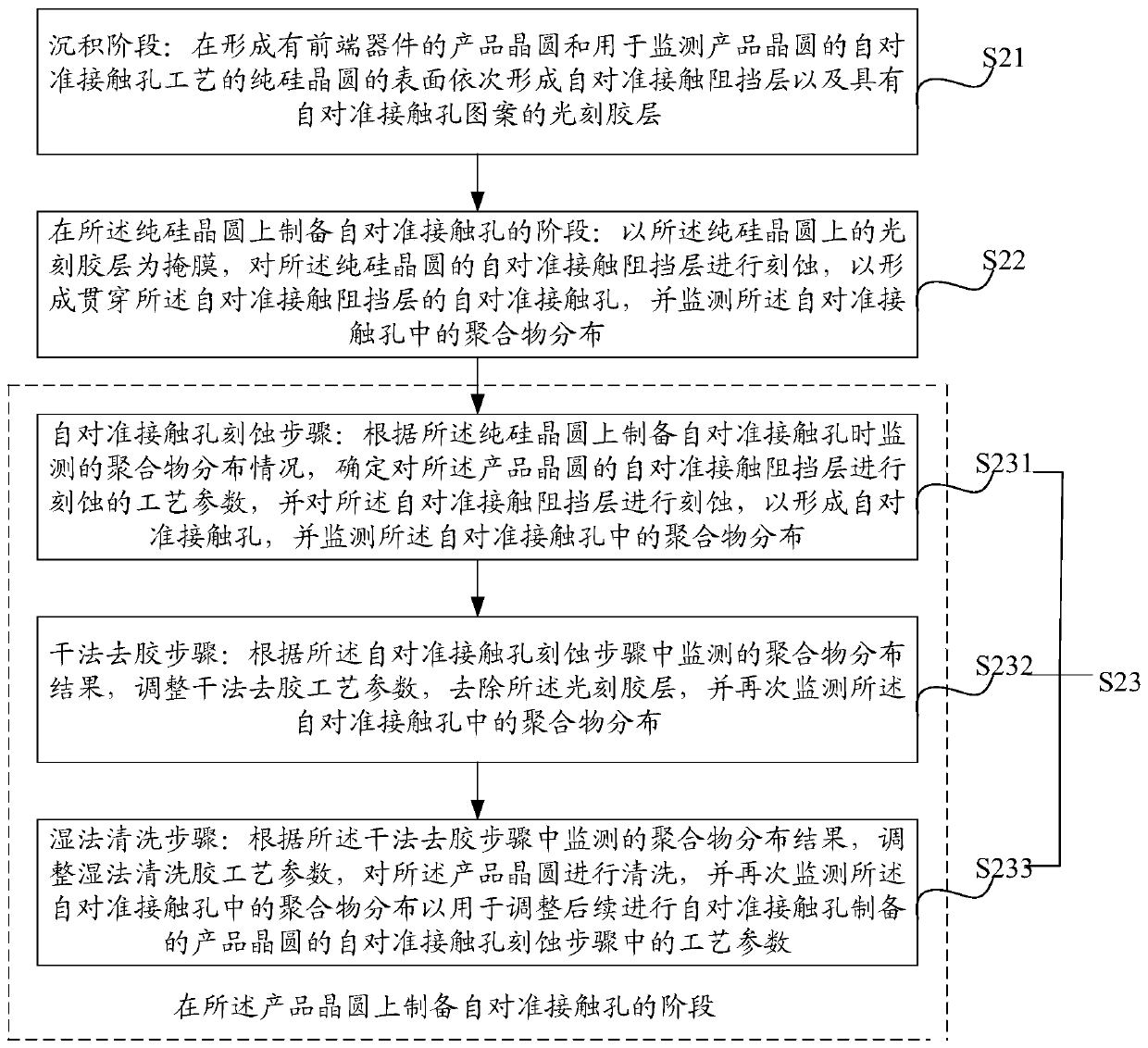
[0030] Please refer to figure 2 , this embodiment provides a method for preparing a self-aligned contact hole, including:

[0031] S21, deposition stage: sequentially form a self-aligned contact barrier layer and a barrier layer with A photoresist layer for self-aligned contact hole patterns;

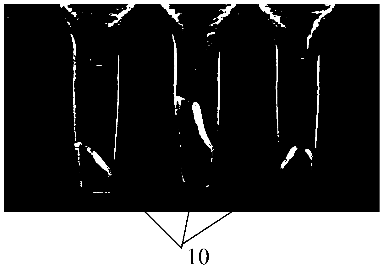
[0032] S22, the stage of preparing a self-aligned contact hole on the pure silicon wafer: using the photoresist layer on the pure silicon wafer as a mask, using a fluorocarbon gas with a fluorocarbon ratio not greater than 2 to treat the The self-aligned contact barrier layer of the pure silicon wafer is etched until the surface of the pure silicon wafer is exposed, so as to form a self-aligned contact hole penetrating through the self-aligned contact barrier layer, and monitor the Polymer distribution in self-aligned contact holes;

[0033] S23, the stage of preparing self-aligned contact holes on the product wafer, including:

[0034] S231, self-aligned contact hole etching step: u...

Embodiment 2

[0048] Please refer to Figure 4 , this embodiment provides a method for preparing a self-aligned contact hole, including:

[0049] S41, deposition step: sequentially forming a doped silicon oxide glass layer, a protective oxide layer, and a photoresist layer with a self-aligned contact hole pattern on the surface of the substrate wafer;

[0050] S42, the initial etching step of the self-aligned contact hole: using the photoresist layer as a mask, etching the protective oxide layer to the surface of the doped vitreous silica layer, so as to form the protective oxide layer through the and monitoring the polymer distribution in the openings of the protective oxide layer;

[0051] S43, dry stripping step: according to the polymer distribution result in the opening of the protective oxide layer, adjust the parameters of the dry stripping process, remove the photoresist layer, and monitor again the polymer in the self-aligned contact hole polymer distribution;

[0052] S44, self...


PUM


Abstract

The invention provides a fabrication method of a self-alignment contact hole. Monitoring and control on a polymer distribution condition are implemented in each stage of etching, photoresist removal by a dry method and cleaning by a wet method of a self-alignment contact hole process, the polymer distribution condition collected after a previous step is fed back to a process formula in a next step, so that relatively high removal rate / etching rate, favorable removal uniformity, controllable side-wall morphology and feature size of an opening and the contact hole and low damage to a lower film layer and the like in the next step are achieved, the process effect after the next step is greatly improved, the etching uniformity of the self-alignment contact hole can be further ensured, excessive polymer residue in the self-alignment contact hole in an edge region of a wafer is avoided, and the electrical property and the yield of a device are improved.

Description

technical field [0001] The invention relates to the field of semiconductor manufacturing, in particular to a method for preparing a self-aligned contact hole. Background technique [0002] In the field of semiconductor technology, as the process node of semiconductor technology shrinks continuously, the size of the contact hole (CT) becomes smaller and smaller. Generally, for ordinary devices, self-aligned contact hole (SAC) technology is required when adopting the technology of the process node below 28nm; while for storage devices such as flash memory (Flash), when the technology of the process node below 45nm is used, it is necessary to use self-aligned contact hole (SAC) technology. Self-aligned contact (SAC) technology is adopted. The existing self-aligned contact hole process is usually as follows: After depositing a covering self-aligned contact barrier layer on the front-end device and its gate structure, a mask layer with a self-aligned contact pattern, such as a p...

Claims


Application Information

Patent Timeline
Patent Type & Authority Patents(China)
IPC IPC(8): H01L21/768H01L21/66
CPCH01L21/76897H01L22/26
Inventor 陈宏许昕睿
Owner SHANGHAI HUAHONG GRACE SEMICON MFG CORP
Why Eureka
Try Eureka