Substrate transfer method for vertically structured power semiconductor devices

A power semiconductor, vertical structure technology, applied in the fields of semiconductor devices, semiconductor/solid-state device manufacturing, electric solid-state devices, etc., can solve the problems affecting the cut-off frequency of the device, the decrease of electron mobility, and the reliability degradation of GaN devices, and achieve obvious innovation. performance and research value, simple operation, and the effect of eliminating self-heating effects

Inactive Publication Date: 2017-01-04
CHENGDU HIWAFER SEMICON CO LTD
View PDF10 Cites 1 Cited by
  • Summary
  • Abstract
  • Description
  • Claims
  • Application Information

AI Technical Summary

Problems solved by technology

However, GaN power devices on Si substrates still encounter some bottleneck problems: on the one hand, for example, in the application of high current and high voltage, a strong self-heating effect is generated, which greatly increases the power consumption of the device; on the other hand, The performance of high-power Si-based GaN radio frequency devices decreases with the increase of operating temperature, which affects the device cut-off frequency and leads to the degradation of the reliability of GaN devices.

Method used


Image

  • Substrate transfer method for vertically structured power semiconductor devices

Examples


Embodiment Construction

[0020] The following will clearly and completely describe the technical solutions in the embodiments of the present invention with reference to the accompanying drawings in the embodiments of the present invention. Obviously, the described embodiments are only part of the embodiments of the present invention, not all of them. Based on the embodiments of the present invention, all other embodiments obtained by persons of ordinary skill in the art without making creative efforts belong to the protection scope of the present invention.

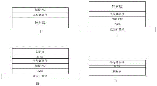
[0021] Provide a kind of substrate transfer method of vertical structure power semiconductor device, it is characterized in that, comprising the steps:

[0022] Step 1: Coating a layer of polyimide on the upper surface of the original GaN power semiconductor device as a protective layer of the GaN device, and putting it into a vacuum oven for curing;

[0023] Step 2: Coating a paraffin layer on top of the cured polyimide layer, and bonding the pa...


PUM

PropertyMeasurementUnit
Thicknessaaaaaaaaaa
Thicknessaaaaaaaaaa

Abstract

The invention provides a substrate transfer method for vertically structured power semiconductor devices. A GaN power semiconductor device arranged on a Si-based substrate is transferred to a target Cu substrate by a special wafer level bonding technology. The method is a brand new substrate transfer technology, a Cu substrate with large thermal conductivity coefficient can effectively help the GaN power semiconductor device to cool, eliminate the self-heating effect of a high power transistor, and simultaneously reduce the power consumption of the GaN power device and improve the reliability of equipment at high temperature. The method is simple to operate, can promote the application of the GaN device in the next-generation millimeter-wave radar transmitter / receiver components (T / R) and complex aerospace fields, and has obvious innovativeness and research value.

Description

technical field [0001] The invention relates to a brand-new substrate transfer method for a power semiconductor device with a vertical structure, belonging to the field of semiconductor manufacturing. Background technique [0002] Silicon-based chips have experienced decades of development. As the size of Si-based CMOS continues to shrink, its frequency performance has also continued to improve. It is expected that when the feature size reaches 25nm, its f T Up to 490GHz. However, the Johnson figure of merit of Si material is only 0.5 THzV, and the breakdown voltage of Si CMOS devices will be much smaller than 1V when the size is reduced, which greatly limits the application of silicon-based chips in the ultra-high-speed digital field. In recent years, people are constantly looking for its substitutes. Since the wide bandgap semiconductor gallium nitride (GaN) material has an ultra-high Johnson figure of merit (5 THzV), when the device channel size reaches the order of 10nm...

Claims


Application Information

Patent Timeline
IPC IPC(8): H01L21/02H01L21/683H01L21/78
CPCH01L21/02016H01L21/02019H01L21/02697H01L21/6835H01L21/7813H01L2221/68386
Inventor 黎明
Owner CHENGDU HIWAFER SEMICON CO LTD
Why Eureka
Try Eureka