A kind of etching method of tantalum nitride tan film

A tantalum nitride and thin film technology, which is applied in the etching field of tantalum nitride and TaN thin film, can solve the problems of reducing product yield, affecting the compatibility of etching process, aggravating damage, etc., and achieving the effect of uniform etching rate

Active Publication Date: 2019-02-22
ADVANCED MICRO FAB EQUIP INC CHINA
View PDF4 Cites 0 Cited by
  • Summary
  • Abstract
  • Description
  • Claims
  • Application Information

AI Technical Summary

Problems solved by technology

Therefore, during the etching process, due to the inhomogeneity and anisotropy of the etching rate on the entire film, there will be over-etching in some areas, especially the grain boundary area, and due to the inhomogeneity and anisotropy The rate will further deteriorate as the process progresses in the etch
The over-etching phenomenon will cause the etching of the film under the TaN film, thereby transferring the etching damage to the underlying structure, and the damage will be further aggravated due to the bombardment of ions
Uneven etching and damage to the underlying film will affect the compatibility of the etching process and greatly reduce the product yield

Method used


Image

  • A kind of etching method of tantalum nitride tan film
  • A kind of etching method of tantalum nitride tan film
  • A kind of etching method of tantalum nitride tan film

Examples


Embodiment Construction

[0027] In order to make the object and technical effect of the present invention more clear and complete, the specific implementation manners of the present invention will be described below in conjunction with the accompanying drawings.

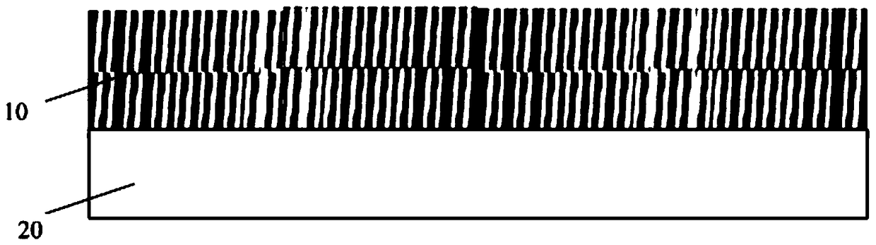
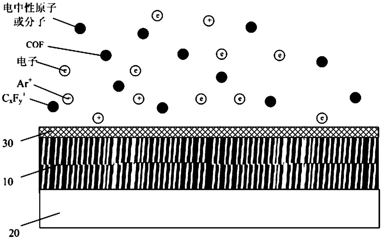
[0028] figure 1 is a schematic diagram of the structure of a TaN thin film with a crystalline structure containing columnar crystals. from the figure 1 It can be seen that the internal microstructure of the TaN thin film 10 is not uniform. Its inhomogeneous microstructure leads to different etching rates in different regions of the TaN film. And the etch rate at the grain boundary or crystal defect is too fast. This leads to over-etching at grain boundaries or at crystallographic defects when other regions are fully etched. The occurrence of over-etching and the enhancement of ion bombardment at the defect will transfer the defect of the TaN film to the film structure 20 below it, forming a defect that will affect the performance of the ...


PUM


Abstract

The invention provides an etching method of tantalum nitride TaN film, comprising the steps of a, in a first period, introducing first etching gas into a reaction chamber such that TaN and the first etching gas engage in interfacial reaction to generate a first etching product; b, in a second period, introducing second etching gas into the reaction chamber; c, cyclically executing the steps a and b until TaN is completely removed; in the TaN etching method provided herein, it can be guaranteed in the whole etching process that different areas of the TaN film are at uniform etching rate, and therefore after etching of the whole TaN film material, both cases are avoided that a local area experiences over-etching and the layer structure below the TaN film is damaged by over-etching. Therefore, compared with the prior etching method, the etching method provided herein can provide increased compatibility for the etching process and increased yield for products.

Description

technical field [0001] The invention relates to the field of semiconductor processing technology, in particular to an etching method for a tantalum nitride TaN thin film. Background technique [0002] In deep submicron integrated circuits, tantalum nitride (TaN) is a commonly used material layer in metal interconnect structures. This is because tantalum nitride is currently the ideal diffusion barrier material for preventing metal diffusion. [0003] In the process of depositing thin films, reactive ion sputtering (Reactive Ion Sputtering) is a common method for preparing TaN (tantalum nitride) thin films. However, due to the characteristics of the sputtering deposition process, the TaN thin film is mainly composed of columnar structure grains of tantalum fluoride chemical components in various chemical states, and there are intercrystalline regions of amorphous state and chemical composition segregation between the grains. XRD detection shows that the TaN film deposited b...

Claims


Application Information

Patent Timeline
Patent Type & Authority Patents(China)
IPC IPC(8): H01L21/311H01L21/768
CPCH01L21/31138H01L21/76865H01L2221/1073
Inventor 刘骁兵刘志强
Owner ADVANCED MICRO FAB EQUIP INC CHINA
Why Eureka
Try Eureka