

A kind of semiconductor device and its manufacturing method and electronic device
A technology for a semiconductor and a manufacturing method, which is applied in the fields of semiconductor devices and their manufacturing methods and electronic devices, can solve problems such as poor flatness, and achieve the effects of good performance, good surface flatness, and avoidance of residues
- Summary
- Abstract
- Description
- Claims
- Application Information
AI Technical Summary
Problems solved by technology
Method used
Image

Examples
Embodiment Construction
[0033] In the following description, numerous specific details are given in order to provide a more thorough understanding of the present invention. It will be apparent, however, to one skilled in the art that the present invention may be practiced without one or more of these details. In other examples, some technical features known in the art are not described in order to avoid confusion with the present invention.
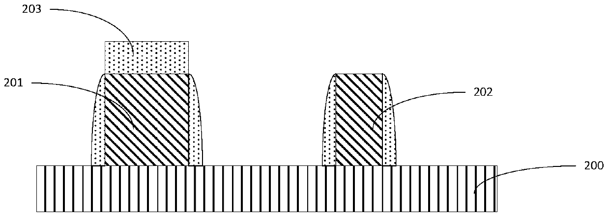
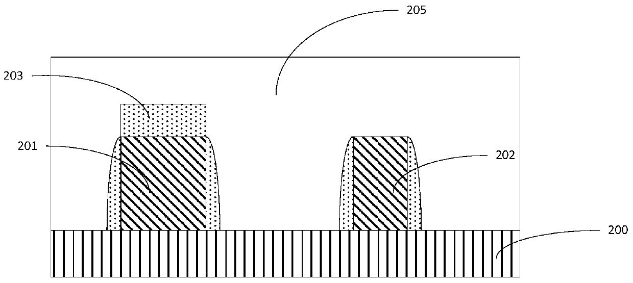
[0034] It should be understood that the invention can be embodied in different forms and should not be construed as limited to the embodiments set forth herein. Rather, these embodiments are provided so that this disclosure will be thorough and complete, and will fully convey the scope of the invention to those skilled in the art. In the drawings, the size and relative sizes of layers and regions may be exaggerated for clarity. Like reference numerals refer to like elements throughout.
[0035] It will be understood that when an element or layer is referred t...
PUM
 Abstract
Description
Claims
Application Information