Asymmetric-structure-based organic semiconductor thin film oriented-preparation method and characterization method

An organic semiconductor and asymmetric structure technology, applied in semiconductor/solid-state device manufacturing, semiconductor devices, test crystals, etc., can solve the problems of device operating speed reduction, slow film formation speed, and inability to meet the needs of orientation growth, etc., to achieve small The effect of parasitic capacitance and fast switching speed

Active Publication Date: 2017-01-25
上海鼎弈材料科技有限公司
View PDF6 Cites 6 Cited by
  • Summary
  • Abstract
  • Description
  • Claims
  • Application Information

AI Technical Summary

Problems solved by technology

[0003] Existing thin film preparation technologies that can control film growth behavior and molecular arrangement include pulling coating technology, solution shearing thin film preparation technology, and some such as using tilted substrates to instill precursor liquid or film orientation preparation based on solution evaporation l

Method used


Image

  • Asymmetric-structure-based organic semiconductor thin film oriented-preparation method and characterization method
  • Asymmetric-structure-based organic semiconductor thin film oriented-preparation method and characterization method
  • Asymmetric-structure-based organic semiconductor thin film oriented-preparation method and characterization method

Examples


Embodiment 1

[0037] Embodiment 1 Utilizes the method for preparing organic semiconductor film by asymmetric planar structure orientation

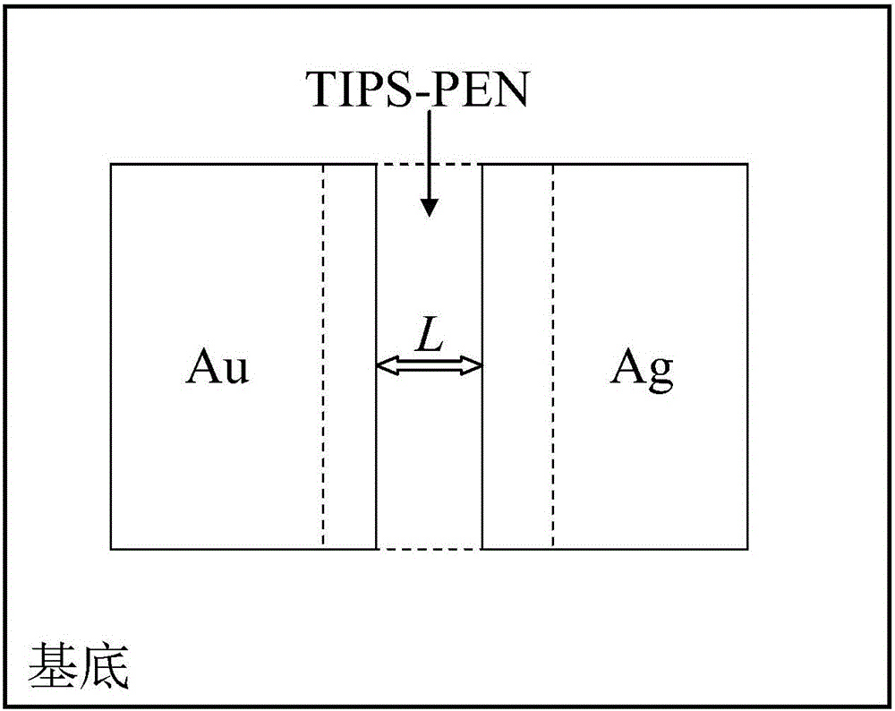
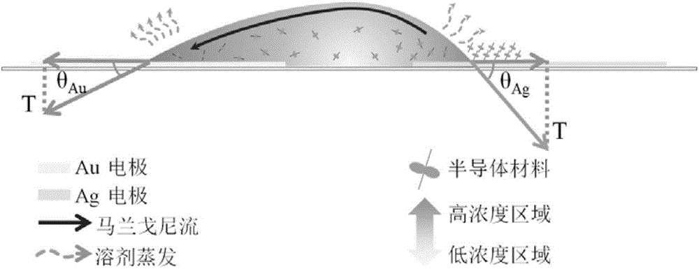
[0038] In this embodiment, the method for preparing an organic semiconductor thin film using an asymmetric planar structure orientation is: take material A and material B, there is a difference in surface energy between the two, and the contact angle between material A and the organic semiconductor precursor solution to be printed is greater than that of material A. The contact angle between B and the organic semiconductor precursor solution to be printed; the patterned films of material A and material B are respectively formed on the substrate, which are respectively film A and film B, and there is a channel in the middle of film A and film B, defining the channel The channel length L is the shortest distance between film A and film B, and the direction corresponding to the channel length is the channel length direction; the precursor solution of the or...

Embodiment 2

[0046] Embodiment 2 Utilizes the method for preparing film by asymmetric stereostructure orientation

[0047] In this embodiment, the method for preparing a thin film using asymmetric stereostructure orientation is as follows: Figure 5 As shown, film C and film D are arranged at intervals on the substrate, and film C and film D are connected by an arc-shaped transition of film E, the thickness of film C is greater than the thickness of film E, and the thickness of film D is greater than or equal to the thickness of film E , the minimum radius of curvature at the joint between film C and film E is smaller than the minimum radius of curvature at the joint between film D and film E; define the spacing direction from film C to film D as the width direction of film E or the channel length direction, and print by inkjet The precursor solution of the organic semiconductor thin film material is printed on the horizontal substrate along the horizontal direction perpendicular to the wi...

Embodiment 3

[0050] The characterization method of the orientation strength of the oriented growth film of embodiment 3

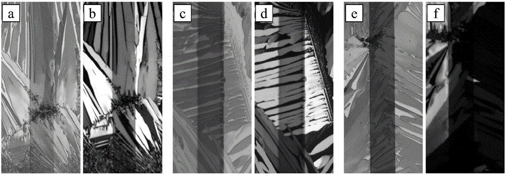
[0051] The characterization method of the orientation strength of the oriented growth film in this embodiment is to characterize the in-plane orientation strength of the oriented growth film through the out-of-plane X-ray diffraction spectrum. The orientation strength includes two quantitative evaluation indicators: the consistency of the orientation growth direction and the degree of orientation growth. Continuity, the specific characterization steps are:

[0052] (1) first determine whether the organic semiconductor film to be characterized is oriented growth through a polarizing microscope, and if so, proceed to step (2);

[0053](2) Define the angle between the X-ray incident surface of out-of-plane X-ray diffraction and the expected growth direction of the organic semiconductor thin film to be characterized as the test azimuth angle α, and take Δα as the change ste...


PUM

PropertyMeasurementUnit
Thicknessaaaaaaaaaa
Thicknessaaaaaaaaaa

Abstract

The invention discloses an asymmetric-structure-based organic semiconductor thin film oriented-preparation method and a characterization method. The oriented-preparation method is characterized in that a semiconductor precursor solution is delivered to a specified position of a substrate in a non-contact material delivery manner by adopting picoliter-level droplets jetted according to requirements and a digital direct writing patterning technology on the basis of a micro-nano inkjet printing technology, and then a guiding function in semiconductor growth is realized to obtain an oriented-growing semiconductor thin film on the basis of the asymmetric surface tension action on the solvent on the substrate and a surface energy gradient formed on the surface thereof. According to the methods, oriented growth of a small-sized inner thin film is realized, and the thin film of which growth orientation and continuity thereof are effectively controlled has an anisotropic optical characteristic and long-range order coherence information, and is expected to be applied to high-frequency organic thin film transistor and array light field sensors.

Description

technical field [0001] The invention relates to a method and a characterization method for oriented growth of an organic semiconductor thin film, belonging to the technical field of printed electronics. Background technique [0002] Printed electronics technology is based on flexible organic material systems and inkjet printing and other solution patterned thin film preparation technologies to produce low-cost electronic products at low temperatures. Among them, the manufacture of organic thin film transistors is one of the key technologies. At present, the mobility of high-mobility organic materials can reach 10cm 2 V -1 the s -1 On the order of magnitude, the development of this class of materials has made printed electronics of devices based on organic thin-film transistors quite broad in potential applications. The current application of organic electronics is mainly limited by its poor high-frequency working ability. The main bottleneck of related technologies is fi...

Claims


Application Information

Patent Timeline
IPC IPC(8): H01L51/40G01N21/84G01N23/20
CPCG01N21/8422G01N23/20G01N2021/8477H10K71/135
Inventor 王向华顾勋吕申宸
Owner 上海鼎弈材料科技有限公司
Why Eureka
Try Eureka