Scanning tunneling microscope probe with use of two-dimensional atomic crystal material

A two-dimensional atomic crystal and scanning tunneling technology, which is applied in the field of scanning tunneling microscope probes, can solve the problems of high material costs, probes that cannot reach the atomic level, and large curvature radius of the tip, etc., and achieve low cost, excellent conductivity, and line Scan the effect of Quick Scan

Active Publication Date: 2017-02-08
SUN YAT SEN UNIV
View PDF7 Cites 4 Cited by
  • Summary
  • Abstract
  • Description
  • Claims
  • Application Information

AI Technical Summary

Problems solved by technology

Tungsten tip probe is the most commonly used STM probe, it has the advantages of stable structure and low manufacturing cost, but it has the disadvantages of large radius of curvature of the tip
Platinum-iridium tip probes are commercial STM probes, which are si

Method used


Image

  • Scanning tunneling microscope probe with use of two-dimensional atomic crystal material
  • Scanning tunneling microscope probe with use of two-dimensional atomic crystal material
  • Scanning tunneling microscope probe with use of two-dimensional atomic crystal material

Examples


Embodiment Construction

[0019] The content of the present invention will be further described below in conjunction with the accompanying drawings and specific embodiments.

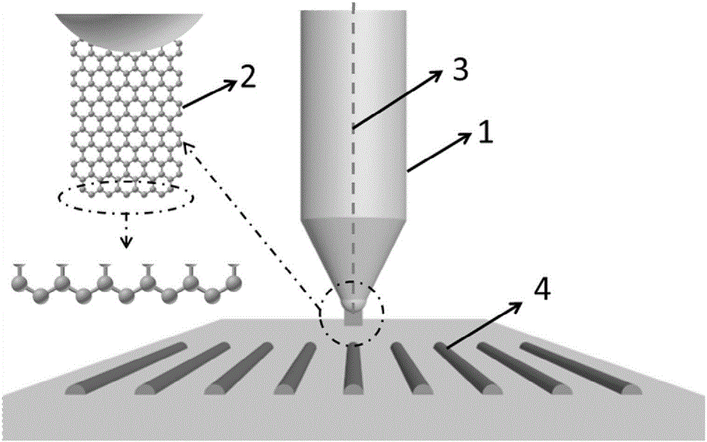
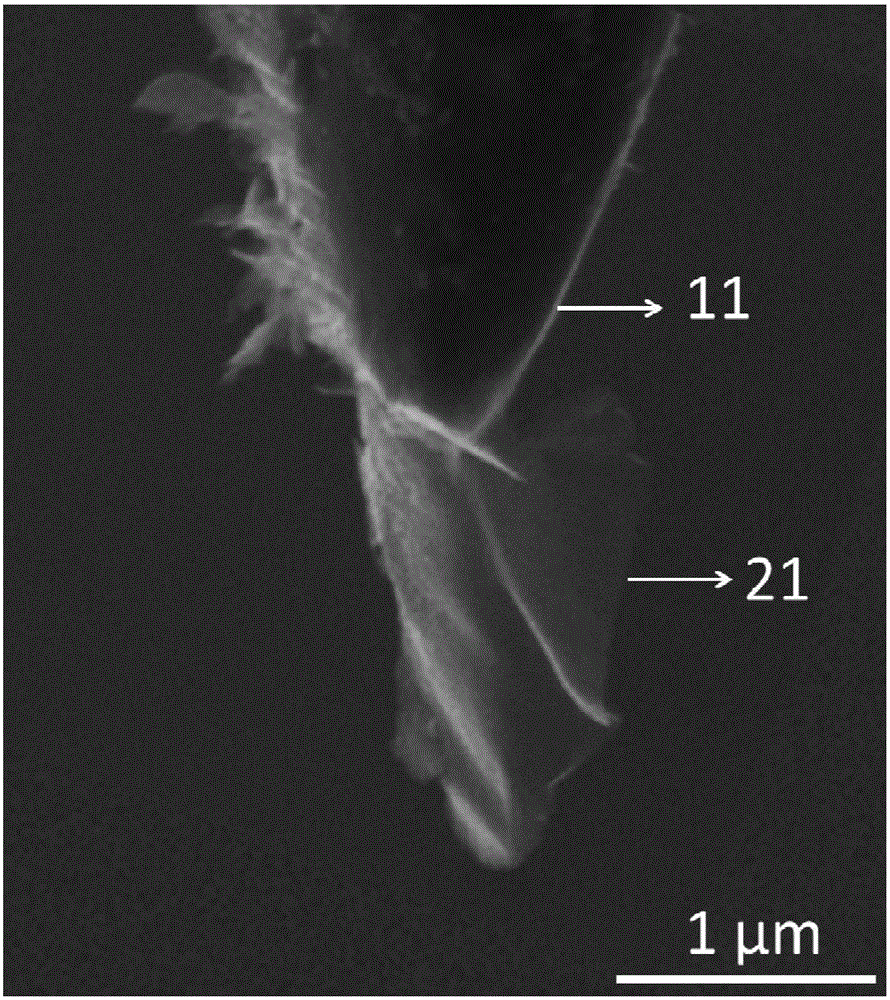
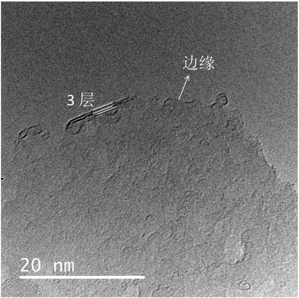
[0020] refer to figure 1 The schematic diagram of the two-dimensional atomic crystal material STM probe structure, the specific implementation steps of the present invention are as follows:

[0021] Step 1: Probe preparation. The two-dimensional atomic crystal material 2 is vertically fixed on the end surface of the conductive rod 1 in the form of ohmic contact to obtain the two-dimensional atomic crystal material STM probe. Wherein, the growth direction of the two-dimensional atomic crystal material 2 is parallel to the axis 3 of the conductive rod.

[0022] Step 2: The probe and the sample to be tested 4 are installed. The two-dimensional atomic crystal material STM probe is loaded into the STM probe holder, the sample 4 to be tested is placed on the STM test bench, and the STM is vacuumed to reach the vacuum required for th...


PUM


Abstract

The invention relates to a scanning tunneling microscope probe with the use of a two-dimensional atomic crystal material. The two-dimensional atomic crystal material is vertically fixed to the end face of a conductive rod according to an ohmic contact mode, an atomic level tip is realized by using the atomic layer thickness of the two-dimensional atomic crystal material, line scanning is obtained by using the linear beam electron emission of a two-dimensional structure, and the high conductivity of the two-dimensional atomic crystal material is used to realize weak signal acquisition. The technical realization method of the invention is simple, and high resolution imaging and rapid scanning imaging functions can be realized.

Description

technical field [0001] The invention relates to a scanning tunneling microscope probe using a two-dimensional atomic crystal material, which can realize high-resolution imaging and fast scanning imaging. The invention belongs to the technical field of scanning tunneling microscopic imaging. Background technique [0002] The basic principle of scanning tunneling microscopy (STM) is to apply a voltage between the pointed probe and the sample to generate a tunneling current, and then use the tunneling current to have an exponential relationship with the probe-sample distance to achieve local detection of the sample, thereby obtaining material Structural information at atomic resolution. This technique is widely used in material structure analysis, surface and microstructure physical phenomena research. [0003] The probe is a key component of STM, which determines the performance of STM imaging resolution, scanning speed and so on. The diameter of the probe tip determines th...

Claims


Application Information

Patent Timeline
IPC IPC(8): G01Q60/16
CPCG01Q60/16
Inventor 邓少芝唐帅张宇许宁生陈焕君陈军佘峻聪
Owner SUN YAT SEN UNIV
Why Eureka
Try Eureka