Ga2O3-material-based U-shaped grating type MOSFET and preparation method thereof

A -ga2o3, U-shaped technology, applied in the field of Ga2O3-based U-shaped gate MOSFET and its preparation, can solve the problems of large on-resistance, high cost, limitations, etc., achieve excellent material characteristics, improve withstand voltage and reverse Effects of breakdown voltage and on-resistance reduction

Inactive Publication Date: 2017-02-22
XIDIAN UNIV
View PDF11 Cites 9 Cited by
  • Summary
  • Abstract
  • Description
  • Claims
  • Application Information

AI Technical Summary

Problems solved by technology

With the application requirements in extreme environments such as deep space exploration, deep oil and gas exploration, ultra-high voltage power conversion, high-speed locomotive drive, and nuclear energy development, Si-based power devices can no longer meet the requirements of high power, high frequency, and high temperature. In addition, Si-based power devices The large on-resistance of the device also greatly reduces the energy conversion efficiency of the system, and the demand for high-performance and high-power devices is becoming more and more urgent
[0003] At present, it is more common to apply wide bandgap materials 4H-SiC, 6H-SiC, etc. to MOS power devices, and some of them have been put into commercial application, which greatly improves the withstand voltage and reverse breakdown electric field of the device, and is more suitable for high temperature and high voltage. In extreme environments such as high frequency and high radiation, the reliability of the device is improved, but due to the complicated preparation process of 4H-SiC and 6H-SiC single crystal, the high cost limits the application of this material

Method used


Image

  • Ga2O3-material-based U-shaped grating type MOSFET and preparation method thereof
  • Ga2O3-material-based U-shaped grating type MOSFET and preparation method thereof
  • Ga2O3-material-based U-shaped grating type MOSFET and preparation method thereof

Examples


Embodiment 1

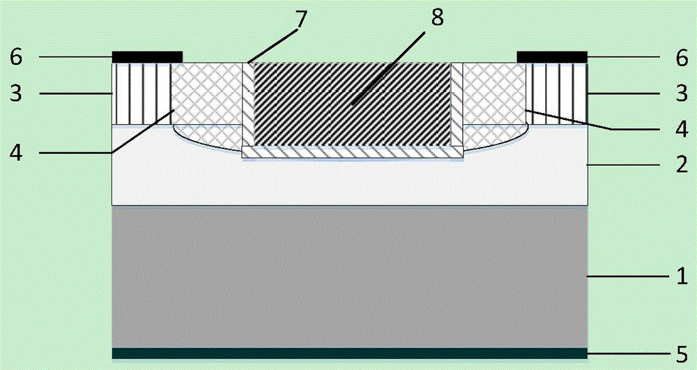
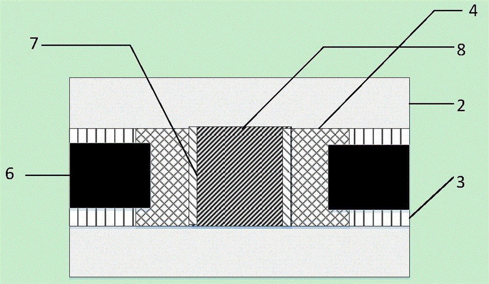
[0052] See figure 1 and figure 2 , figure 1 Provided for an embodiment of the present invention based on Ga 2 O 3 Cross-sectional schematic diagram of U-gate MOSFET of material, figure 2 Provided for an embodiment of the present invention based on Ga 2 O 3 A schematic top view of a U-gate MOSFET made of materials. The U-shaped gate MOSFET of the present invention includes: a substrate 1, a homoepitaxial layer 2, an N-type doped region 3, a P well region 4, a drain electrode 5, a source electrode 6, a gate oxide layer 7, and a gate electrode 8.

[0053] The substrate has a doping concentration of 10 18 -10 19 cm -3 , N-type β-Ga with doping elements such as Sn, Si, Al, etc. 2 O 3 (-201), N-type β-Ga 2 O 3 (010) or N type β-Ga 2 O 3 (001) Material; The homoepitaxial layer is β-Ga with the same doping element as the substrate material 2 O 3 , Doping concentration 10 15 cm -3 Magnitude; the doping element in the N-type doped region can be Sn, Si, Al and other elements, and the doping...

Embodiment 2

[0091] See also Figure 4a-Figure 4i and Figure 5 to Figure 8 , Figure 4a-Figure 4h Provides a Ga-based 2 O 3 Schematic diagram of the preparation method of U-gate MOSFET made of materials; Figure 5 Is a schematic structural diagram of a first mask provided by an embodiment of the present invention; Image 6 Is a schematic structural diagram of a second mask provided by an embodiment of the present invention; Figure 7 Is a schematic structural diagram of a third mask provided by an embodiment of the present invention; and Picture 8 This is a schematic structural diagram of a fourth mask provided by an embodiment of the present invention. In this embodiment, on the basis of the above embodiment, the method for preparing the U-gate MOSFET of the present invention is described in detail as follows:

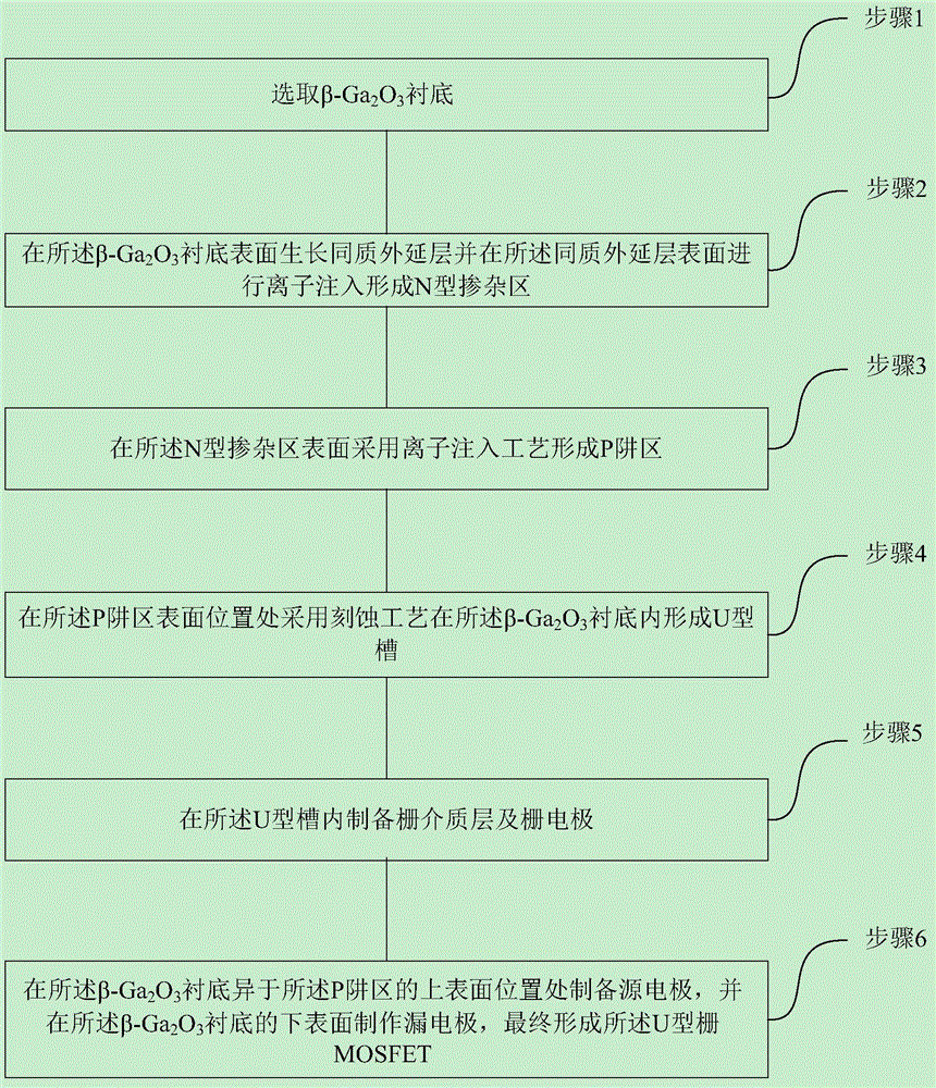
[0092] Step 1: See Figure 4a , Prepare β-Ga 2 O 3 Substrate 1, the substrate doping concentration is 10 18 -10 19 cm -3 , The thickness is 200μm-600μm, and the substrate is pretreat...


PUM


Abstract

The invention relates to a Ga2O3-material-based U-shaped grating type MOSFET and a preparation method thereof. The method comprises steps: selecting a beta-Ga2O3 substrate; growing a homogeneous epitaxial layer on the surface of the beta-Ga2O3 substrate and carrying out ion implantation on the surface of the homogeneous epitaxial layer to form an N type doped region; carrying out treatment on the surface of the N type doped region by using an ion implantation process to form a P type well region; carrying out treatment on the surface of the P type well region by using an etching process to form a U-shaped groove in the beta-Ga2O3 substrate; preparing a gate dielectric layer and a gate electrode in the U-shaped groove; and preparing a source electrode on the upper surface, different from the P type well region, of the beta-Ga2O3 substrate and manufacturing a drain electrode on the lower surface of the beta-Ga2O3 substrate, thereby forming a U-shaped grating type MOSFET. According to the Ga2O3-material-based U-shaped grating type MOSFET provided by the invention, with the U-shaped grate electrode structure, a high on-resistance defect of the MOSFET power device is overcome; and the Ga2O3 material is applied to the substrate and the homogeneous epitaxial layer of the U-shaped grating structure, so that the voltage-withstanding capability and the reverse breakdown voltage of the MOSFET power device are improved; and the on resistance is reduced and the performance and device reliability of the power device are improved substantially.

Description

Technical field [0001] The invention belongs to the field of integrated circuit technology, and specifically relates to a Ga 2 O 3 Material U-shaped gate MOSFET and its preparation method. Background technique [0002] With the rapid development of electronic technology, power electronics technology, as an important part of energy conversion, has gradually been widely used in industrial production, power systems, transportation, national defense and military, new energy systems, and daily life. As the foundation and core of power electronics technology, the performance of power devices plays an important role in improving the overall system efficiency. They are mainly used in main circuits such as frequency conversion, buck-boost, rectifier and inverter, and power correction. Among them, power devices suitable for extreme environments such as high temperature, high frequency, high pressure, and high radiation have attracted more attention and research. Wide band gap materials suc...

Claims


Application Information

Patent Timeline
Patent Type & Authority Applications(China)
IPC IPC(8): H01L21/34H01L29/78H01L29/22H01L29/423
CPCH01L29/66969H01L29/22H01L29/42356H01L29/7828
Inventor 贾仁需张弘鹏元磊张玉明
Owner XIDIAN UNIV
Why Eureka
Try Eureka