A photoconductive organic semiconductor detector and its preparation method

An organic semiconductor and detector technology, applied in the field of photoconductive organic semiconductor detectors and their preparation, can solve problems such as high dark current and high mobility of materials, and achieve improved detection ratio and switching speed, high switching ratio and responsivity, The effect of increasing distance

Active Publication Date: 2019-05-14
SOUTH CHINA UNIV OF TECH
View PDF3 Cites 0 Cited by
  • Summary
  • Abstract
  • Description
  • Claims
  • Application Information

AI Technical Summary

Problems solved by technology

[0003] In order to overcome the above-mentioned shortcomings and deficiencies of the prior art, the purpose of the present invention is to provide a photoconductive organic semiconductor detector, which solves the problem of large dark current of the existing organic semiconductor detector and breaks through the high sensitivity of the photoconductive detector to materials. Limitation of mobility; it has the advantages of simple structure, high detection ratio, fast response speed, etc. It has important application value and economic value in military, civilian and some specific fields

Method used


Image

  • A photoconductive organic semiconductor detector and its preparation method
  • A photoconductive organic semiconductor detector and its preparation method
  • A photoconductive organic semiconductor detector and its preparation method

Examples


Embodiment 1

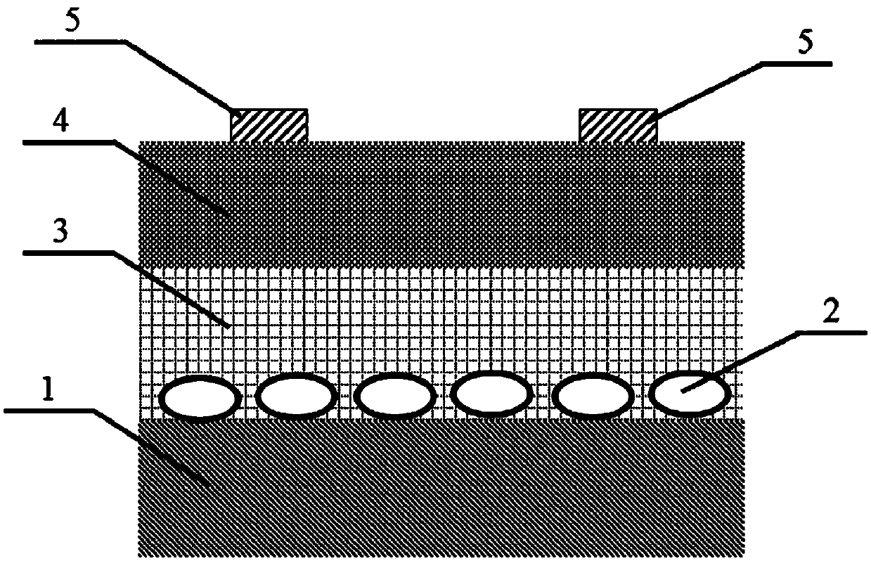
[0050] Such as figure 1 As shown, the photoconductive organic semiconductor detector of this embodiment is formed by stacking a quartz wafer substrate 1, metal nanoparticles 2, an organic insulating layer 3, an organic photosensitive layer 4 and a metal electrode 5 from bottom to top; The absorption peak position of the metal nanoparticles matches the absorption peak position of the organic photosensitive layer to generate localized plasmon resonance.

[0051] The preparation process of the photoconductive organic semiconductor detector of this embodiment is as follows:

[0052] 1. The quartz substrate was soaked in deionized water, acetone, deionized water, ITO cleaning solution, deionized water and isopropanol for 30 minutes, and then placed in an oven at 80°C for drying.

[0053] 2. Plasma treatment was carried out under an oxygen atmosphere for 4 minutes on a clean quartz substrate surface, and the oxygen flow rate during the Plasma process was 4-5mL / s.

[0054] 3. Metal...

Embodiment 2

[0068] The photoconductive organic semiconductor detector of the present embodiment adopts PTB7:PC except the organic photosensitive layer 60 Except for the BM material, other features are the same as in Embodiment 1.

[0069] The preparation method of the organic photosensitive layer of the present embodiment is as follows:

[0070] The organic photosensitive layer was prepared by spin-coating on the substrate with PMMA layer. The organic photosensitive layer uses PTB7:PC 60 BM (2:1-20:1wt%), the solvent is chlorobenzene (CB), and the concentration of the organic photosensitive material is 2wt%. A 100 nm organic photosensitive layer was spin-coated at a rotation speed of 3000 rpm for 30 min. Afterwards, the sample was placed in a vacuum chamber and evacuated for 2 hours to ensure that the solvent was completely removed.

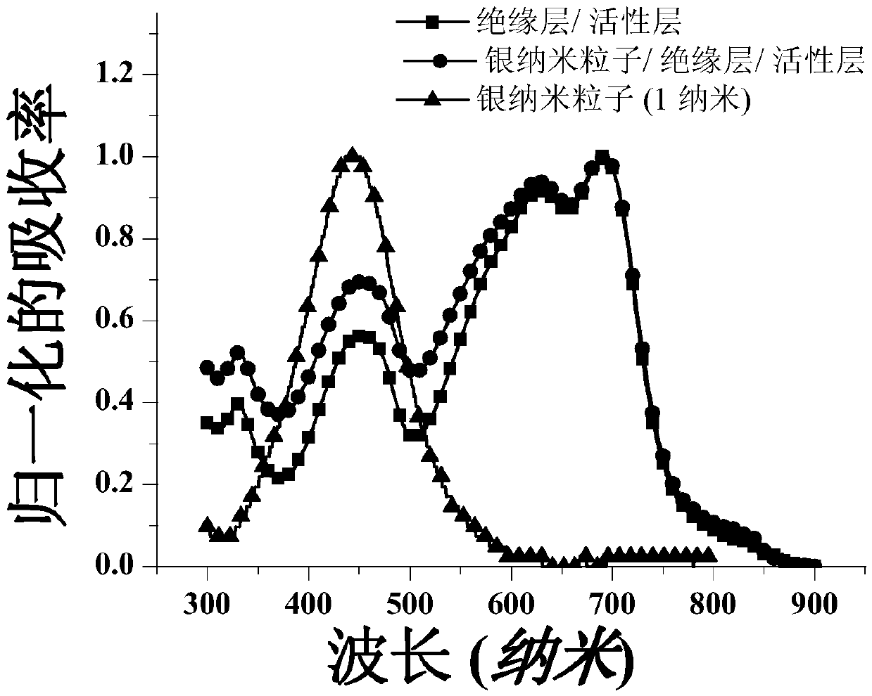
[0071] Figure 11 For Ag nanoparticles, quartz / PMMA / PTB7:PC 60 BM(2:1wt%) / Ag electrode and quartz / Ag nanoparticles / PMMA / PTB7:PC 60Absorption peaks of...

Embodiment 3

[0076] The photoconductive organic semiconductor detector of the present embodiment adopts PffBT4T-2OD:PC except that the organic photosensitive layer 71 Except for the BM material, other features are the same as in Embodiment 1.

[0077] The preparation method of the organic photosensitive layer of the present embodiment is as follows:

[0078] The organic photosensitive layer was prepared by thermal spin coating on the substrate with PMMA layer. Organic photosensitive layer selects PffBT4T-2OD: PC 71 BM (1:1.2-10:1wt%), the solvent is chlorobenzene / dichlorobenzene (CB / DCB (1:1))+3% DIO, and the concentration of the organic photosensitive material is 0.9wt%. Before the thermal spin coating, place the solution and the substrate spin-coated with the PMMA layer on a hot stage for heating at 110°C for 30 minutes, and then spin-coat a 120nm organic photosensitive layer with a rotation speed of 1000 rpm for 30 minutes. The entire thermal spin coating process takes 2 minutes Fini...


PUM


Abstract

The invention discloses a photoconductive organic semiconductor detector, which is formed by stacking a quartz plate substrate, metal nanoparticles, an organic insulating layer, an organic photosensitive layer and a metal electrode from bottom to top; the metal nano particles and the organic photosensitive layer produce localized plasmon resonance. The invention also discloses a preparation method of the photoconductive organic semiconductor detector. The invention solves the problem of large dark current in existing organic semiconductor detectors and breaks through the limitation of photoconductive detectors on the high mobility of materials. The photoconductive organic semiconductor detector of the invention has the advantages of simple structure, high detection ratio, fast response speed, etc., and has important application value and economic value in military, civil and some specific fields.

Description

technical field [0001] The invention relates to an organic semiconductor detector, in particular to a photoconductive organic semiconductor detector and a preparation method thereof. Background technique [0002] Optical detectors are widely used in the fields of optical communication, remote control devices and image sensing, and low noise, high quantum efficiency, large detection ratio and fast response speed are important indicators to measure the performance of detectors. Traditional photodetectors are mainly divided into two categories: photovoltaic detectors and photoconductive detectors. At present, the main research in organic materials is photovoltaic organic semiconductor detectors. Its short electrode distance (≈100nm) can ensure that the carriers in the organic photosensitive materials can quickly move to the electrodes, which makes the disadvantages of low mobility of organic materials. It can be compensated, but at the same time, the short electrode distance b...

Claims


Application Information

Patent Timeline
Patent Type & Authority Patents(China)
IPC IPC(8): H01L51/42H01L51/46H01L51/48
CPCH10K85/00H10K30/00H10K2102/00Y02E10/549
Inventor 刘琳琳马於光解增旗韩滔
Owner SOUTH CHINA UNIV OF TECH
Why Eureka
Try Eureka