Four-wavelength output semiconductor laser device and preparation method thereof

A semiconductor and laser technology, applied in the field of four-wavelength output semiconductor lasers and their preparation, can solve problems such as inability to transmit signals, and achieve the effects of strong intracavity light field, improved stability and convenience, and improved energy consumption

Active Publication Date: 2017-02-22
INST OF SEMICONDUCTORS - CHINESE ACAD OF SCI
View PDF3 Cites 5 Cited by
  • Summary
  • Abstract
  • Description
  • Claims
  • Application Information

AI Technical Summary

Problems solved by technology

[0004] In addition, due to the limitation of the substrate, GaAs-based lasers are considered unable to emit signals above 1.5 μm, so GaAs-based lasers with the most mature technology cannot be used in the band above 2 μm; and PPLN is used as a nonlinear conversion core device The conversion wavelength range is 0.4-5μm, and there is no way to use it in the band above 5μm, while AlGaAs, as the core device of nonlinear conversion, has a conversion wavelength range of 0.7-17μm, and the second-order nonlinear coefficient is much higher than that of PPLN

Method used


Image

  • Four-wavelength output semiconductor laser device and preparation method thereof
  • Four-wavelength output semiconductor laser device and preparation method thereof
  • Four-wavelength output semiconductor laser device and preparation method thereof

Examples


preparation example Construction

[0086] The invention also discloses a method for preparing a tunable monolithic integrated four-wavelength output semiconductor optical parametric oscillation laser, which includes the following steps:

[0087] Step 1: preparing a GaAs substrate;

[0088] Step 2: On the GaAs substrate, sequentially form an N-type GaAs buffer layer, an N-type AlGaAs / GaAs lower DBR (Distributed Bragg Reflector, a distributed Bragg reflector), an N-type GaAs third lower matching layer, and an N-type AlGaAs second Lower matching layer, N-type GaAs first lower matching layer, AlGaAs lower waveguide layer, InGaAs multi-quantum well active region, AlGaAs upper waveguide layer, P-type GaAs first upper matching layer, P-type AlGaAs second upper matching layer, P Type GaAs third upper matching layer, P-type AlGaAs / GaAs upper DBR, P-type GaAs contact layer.

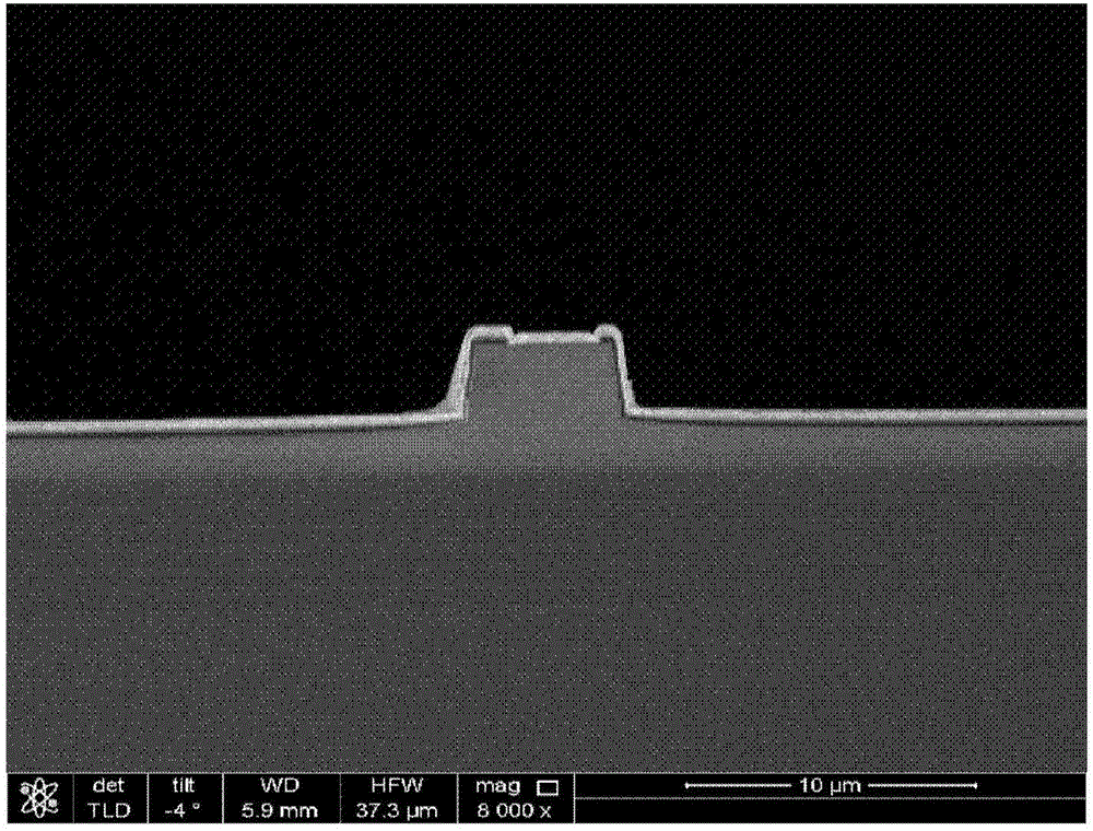
[0089] Step 3: Etching downward from the P-type GaAs contact layer by using photolithography technology and etching technology, and the etching de...


PUM


Abstract

The invention provides a four-wavelength output semiconductor laser device and a preparation method thereof. The laser device is a near-infrared edge-emitting laser device. An existing upper and lower limiting layer structure is replaced with upper and lower DBR bands; and a defect layer is inserted into one-dimensional photonic crystal, so that the effect of limiting light in a photonic band gap on the defect layer is achieved. The four-wavelength output semiconductor laser device specifically comprises a GaAs substrate, a lower DBR layer, a lower matching layer, a lower waveguide layer, an active layer, an upper waveguide layer, an upper matching layer, an upper DBR layer, a contact layer, an insulating layer and a P-type electrode, wherein the upper DBR layer and the contact layer are etched to form a ridge waveguide and a dual-electrode structure. Output of four different wavelengths can be obtained through internal mode matching of the semiconductor laser device; the effects of tuning the wavelength of the laser device and converting the working state of the laser device can be obtained through controlling one terminal electrode; and the device based on the structure simultaneously obtains continuous pulse output of 1.069 microns, 1.353 microns, 1.77 microns and 2.71 microns.

Description

technical field [0001] The invention relates to a near-infrared edge-emitting laser, in particular to a four-wavelength output semiconductor laser and a preparation method thereof. Background technique [0002] Lasers with different wavelengths have their unique application ranges. Lasers in the 1-2μm band are used in laser ranging, laser guidance, coherence research, atmospheric research, medical equipment, optical image processing, laser printers, short-distance optical fiber communications, and long-distance optical fibers. There are important applications in communication. The 2-5μm band can be widely used in civil projects such as air pollution monitoring and gas detection. The band above 5μm is often used in military projects such as photoelectric countermeasures. However, due to the limitation of the laser gain material, the laser wavelength is often limited to a specific wavelength. Other special wavelengths can only be obtained by means of optical parametric conver...

Claims


Application Information

Patent Timeline
Patent Type & Authority Applications(China)
IPC IPC(8): H01S5/343
CPCH01S5/34306H01S5/34346
Inventor 魏思航张宇廖永平倪海桥牛智川
Owner INST OF SEMICONDUCTORS - CHINESE ACAD OF SCI
Why Eureka
Try Eureka