

Method for manufacturing polycrystal perovskite thin film and solar cell device
A solar cell and perovskite technology, applied in the direction of electric solid-state devices, electrical components, semiconductor devices, etc., can solve the problems of many factors affecting the crystallization process, poor film uniformity, and toxic film thickness, etc., to improve process conditions, equipment and Environmental requirements are low, and the effect of improving quality
- Summary
- Abstract
- Description
- Claims
- Application Information
AI Technical Summary
Problems solved by technology
Method used
Image

Examples
preparation example Construction
[0037] (2) Preparation of the hole transport layer 3: Treat the dried substrate with UV-ozone for 5 to 10 minutes, then spin coat the hole transport layer on the substrate, preferably poly(3,4-ethylenedi Oxythiophene)-polystyrene sulfonic acid (referred to as PEDOT:PSS). The mass fraction of PEDOT:PSS solution is 25%. Use a homogenizer to spin coat the solution. The rotating speed is selected at 1000rpm-2000rpm. The homogenization time is 30s-60s. The time is 0.2-0.5 hours, and the film thickness is 25-40nm.
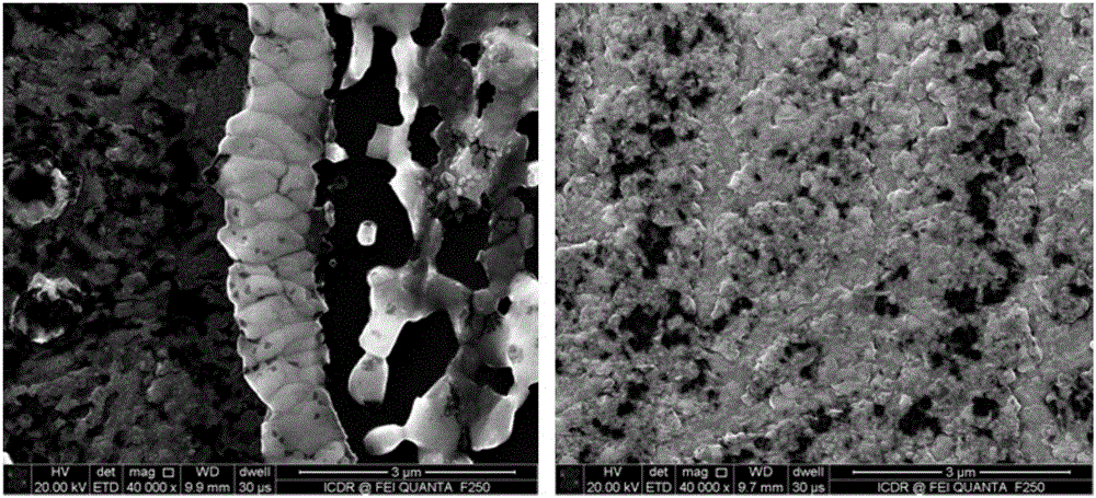
[0038] (3) Preparation of the perovskite thin film 4: prepare the perovskite layer 4 on the hole transport layer 3: prepare the perovskite layer by using the method in the present invention. Among them, the polymer chooses poly(3,4-ethylenedioxythiophene)-poly(styrenesulfonic acid) (referred to as PEDOT:PSS); the salt chooses methyl iodide (referred to as (NH 2 ) 2 CHI), metal halide selective tin iodide (SnI for short 2 ). The first step: the mixed aqueous solution...
Embodiment 1
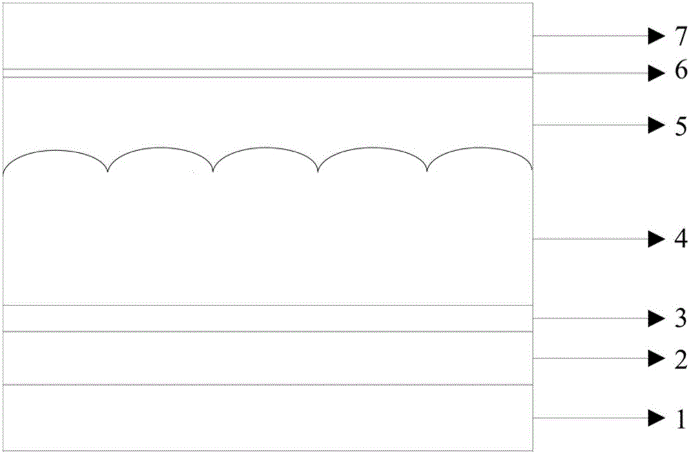
[0044] now refer to figure 1 , the perovskite solar cell device according to the first embodiment of the present invention has the following structure:
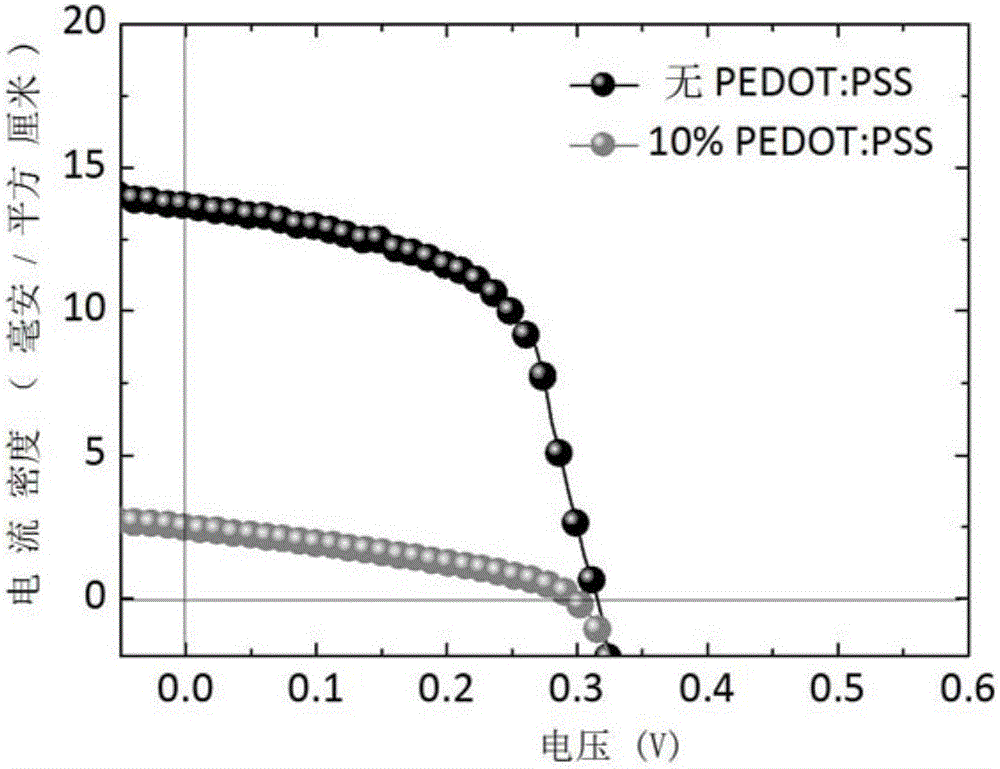
[0045] Glass (plastic) substrate / ITO(100nm) / PEDOT:PSS(30nm) / (NH 2 ) 2 CHSnI 3 (300nm)(10%PEDOT:PSS) / PCBM(8nm) / BCP(10nm) / Ag(120nm)
[0046] (1) Cleaning of glass substrates pre-engraved with ITO: Utilize ethanol, acetone ultrasonic and deionized water ultrasonic methods to clean the transparent conductive substrate 1 (ITO glass), and place it under an infrared lamp to dry after cleaning. Wherein the ITO film on the transparent conductive substrate 1 is used as the anode layer 2 of the device, the square resistance of the ITO film is 15Ω-30Ω, and the film thickness is 80-120nm;
[0047] (2) Preparation of the hole transport layer: Treat the dried substrate with UV-ozone for 5 to 10 minutes, then place it on the KW-4A homogenizer, and use the prepared PEDOT:PSS solution with static batching Method Spin coating to form a fil...
Embodiment 2
[0056] now refer to figure 1 , the perovskite solar cell device according to the second embodiment of the present invention has the following structure:
[0057] Glass (plastic) substrate / ITO(100nm) / PEDOT:PSS(30nm) / (NH 2 ) 2 CHSnI 3 (300nm)(20%PEDOT:PSS) / PCBM(8nm) / BCP(10nm) / Ag(120nm)
[0058] (1) Cleaning of glass substrates pre-engraved with ITO: Utilize ethanol, acetone ultrasonic and deionized water ultrasonic methods to clean the transparent conductive substrate 1 (ITO glass), after cleaning, place it under an infrared lamp to dry, Wherein the ITO film on the transparent conductive substrate 1 is used as the anode layer 2 of the device, the square resistance of the ITO film is 15Ω-30Ω, and the film thickness is 80-120nm;
[0059](2) Preparation of the hole transport layer: Treat the dried substrate with UV-ozone for 5 to 10 minutes, then place it on the KW-4A homogenizer, and use the prepared PEDOT:PSS solution with static batching Method Spin coating to form a film, ...
PUM
| Property | Measurement | Unit |
|---|---|---|
| thickness | aaaaa | aaaaa |
| thickness | aaaaa | aaaaa |
| thickness | aaaaa | aaaaa |
Abstract
Description
Claims
Application Information