Epitaxial wafer for GaN-based light-emitting diode, and growth method for epitaxial wafer

A technology of light-emitting diodes and a growth method, which is applied to the epitaxial wafer of GaN-based light-emitting diodes and its growth field, can solve the problems of high fragmentation rate, lattice mismatch, large thermal expansion coefficient, etc. The effect of reducing the temperature difference

Active Publication Date: 2017-05-10
HC SEMITEK ZHEJIANG CO LTD
View PDF4 Cites 12 Cited by
  • Summary
  • Abstract
  • Description
  • Claims
  • Application Information

AI Technical Summary

Problems solved by technology

There is a lattice mismatch between GaN and sapphire, resulting in high-density defects and a large thermal expansion coefficient of the LED epitaxial wafer, resulting in stress that cannot be fully released, and the surface of the epitaxial wafer is uneven. Compared with the traditional 2-inch epitaxial wafer, large-size epitaxial wafers It has higher warpage and higher fragmentation rate, which seriously restricts the development of large-scale epitaxy technology

Method used


Image

  • Epitaxial wafer for GaN-based light-emitting diode, and growth method for epitaxial wafer
  • Epitaxial wafer for GaN-based light-emitting diode, and growth method for epitaxial wafer
  • Epitaxial wafer for GaN-based light-emitting diode, and growth method for epitaxial wafer

Examples


Embodiment 1

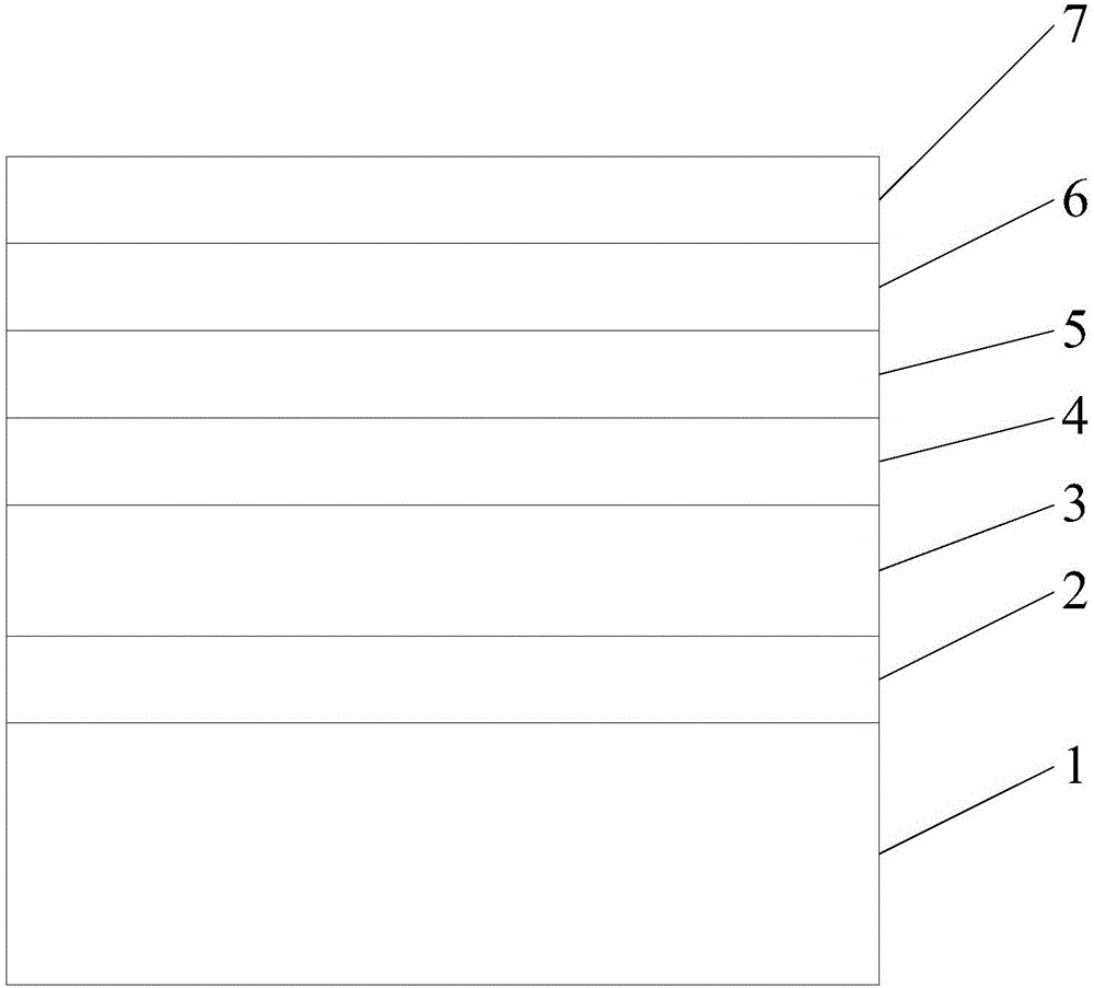
[0029] An embodiment of the present invention provides an epitaxial wafer of a GaN-based light emitting diode, see figure 1 , the epitaxial wafer includes a sapphire substrate 1, and a buffer layer 2, an undoped GaN layer 3, a stress release layer 4, an N-type layer 5, a multi-quantum well layer 6, and a P-type layer stacked sequentially on the sapphire substrate 1. Layer 7.

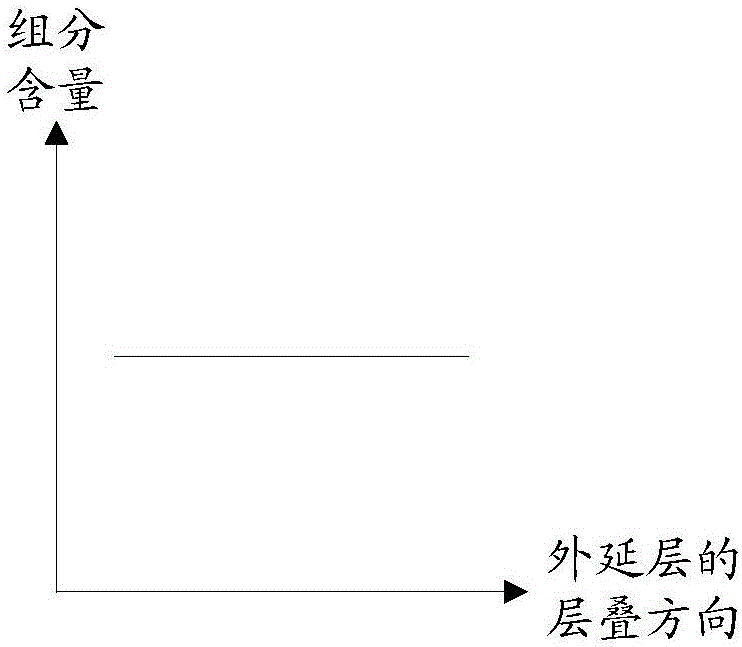
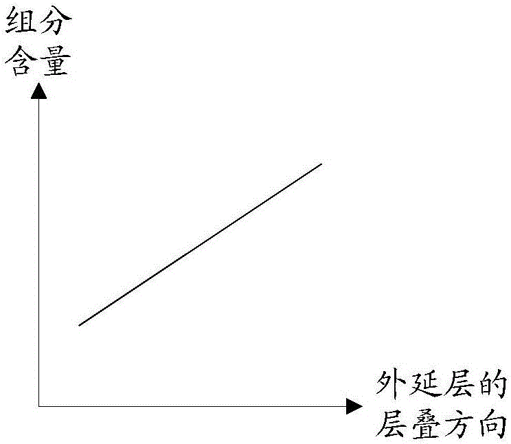
[0030] In this embodiment, the stress release layer includes alternately stacked undoped Al x Ga 1-x N layer and SiN layer, 0≤x Figure 2a shown), linearly increasing along the stacking direction of the epitaxial wafer (such as Figure 2b shown), linearly decreases along the stacking direction of the epitaxial wafer (such as Figure 2c shown), the single layer remains unchanged and increases layer by layer along the stacking direction of the epitaxial wafer (such as Figure 2d shown), the single layer remains unchanged and decreases layer by layer along the stacking direction of the epitaxial wafer (s...

Embodiment 2

[0037] An embodiment of the present invention provides a method for growing an epitaxial wafer of a GaN-based light-emitting diode, which is suitable for growing the epitaxial wafer provided in Embodiment 1, see image 3 , the growth method includes:

[0038] Step 201: Provide a sapphire substrate.

[0039] Step 202: growing a buffer layer, an undoped GaN layer, a stress release layer, an N-type layer, a multi-quantum well layer, and a P-type layer sequentially on the sapphire substrate.

[0040] In this embodiment, the stress release layer includes alternately stacked undoped Al x Ga 1-x N layer and SiN layer, 0≤x<1. The Si component content in the SiN layer changes in any of the following ways: remains constant, increases linearly along the stacking direction of the epitaxial wafers, decreases linearly along the stacking direction of the epitaxial wafers, remains constant for a single layer and increases along the stacking direction of the epitaxial wafers. The direction...

Embodiment 3

[0049] The embodiment of the present invention provides a method for growing epitaxial wafers of GaN-based light-emitting diodes, which is a specific realization of the growth method provided in Embodiment 1, and is realized with high-purity hydrogen (H 2 ) or nitrogen (N 2 ) as carrier gas, trimethylgallium (TMGa), trimethylaluminum (TMAl), trimethylindium (TMIn) and ammonia (NH 3 ) as Ga, Al, In and N sources respectively, with silane (SiH 4 ), Magnesium (Cp 2 Mg) as N and P type dopants respectively.

[0050] Specifically, see Figure 4 , the growth method includes:

[0051] Step 301: The temperature of the substrate is first raised to 500°C, then raised to 800°C and stabilized for 30s, then raised to 1000°C and stabilized for 30s, then raised to 1230°C and stabilized for 10 minutes, and then heat-treated in a pure hydrogen atmosphere.

[0052] It should be noted that the purpose of heat treatment is to clean the substrate surface.

[0053] Step 302: Lower the tempera...


PUM

PropertyMeasurementUnit
Thicknessaaaaaaaaaa
Thicknessaaaaaaaaaa

Abstract

The invention discloses an epitaxial wafer for a GaN-based light-emitting diode, and a growth method for the epitaxial wafer, and belongs to the technical field of semiconductors. The epitaxial wafer comprises a sapphire substrate, a buffering layer, a non-doped GaN layer, a stress releasing layer, an N-type layer, a multi-quantum well and a P-type layer. The stress releasing layer comprises a non-doped AlxGa1-xN layer and a SiN layer, which are alternately stacked, wherein x is greater than or equal to zero and less than one. The content of the Si component in the SiN layer changes in any one following mode: remaining unchanged, linearly increasing in a stacking direction of the epitaxial wafer, linearly decreasing in the stacking direction of the epitaxial wafer, enabling a single layer to remain unchanged and firstly increasing in the stacking direction of the epitaxial wafer layer by layer and secondly decreasing in the stacking direction of the epitaxial wafer layer by layer, and enabling a single layer to remain unchanged and firstly decreasing in the stacking direction of the epitaxial wafer layer by layer and secondly increasing in the stacking direction of the epitaxial wafer layer by layer. The epitaxial wafer can improve the warping.

Description

technical field [0001] The invention relates to the technical field of semiconductors, in particular to an epitaxial wafer of a GaN-based light-emitting diode and a growth method thereof. Background technique [0002] Light Emitting Diodes (English: Light Emitting Diodes, referred to as: LED) has the advantages of small size, colorful colors, and long service life. It is a very influential new product in the emerging industry of information optoelectronics. , backlight, toys and other fields. GaN is an ideal material for making LEDs. Group III nitrides represented by GaN are wide-bandgap semiconductors with direct band gaps. They have high thermal conductivity, high luminous efficiency, stable physical and chemical properties, and can achieve P-type or N-type doping. Advantages, the quantum well structure composed of GaN's multi-element alloy InGaN and GaN not only covers the entire visible light region, but also has a high internal quantum efficiency. [0003] Existing Ga...

Claims


Application Information

Patent Timeline
IPC IPC(8): H01L33/32H01L33/06H01L33/02H01L33/00
CPCH01L33/005H01L33/02H01L33/06H01L33/32
Inventor 杨兰万林胡加辉
Owner HC SEMITEK ZHEJIANG CO LTD
Why Eureka
Try Eureka