Eureka AIR delivers breakthrough ideas for toughest innovation challenges, trusted by R&D personnel around the world.

LDMOS with low conduction resistance and relatively low total gate charge and preparation method for LDMOS

A technology with low on-resistance and preparation process, applied in semiconductor/solid-state device manufacturing, circuits, electrical components, etc., can solve low on-resistance and total gate charge, high LDMOS on-resistance and total gate charge, Low on-resistance and other issues, to achieve low total gate charge, good effect of suppressing high electric field, and low on-resistance

Inactive Publication Date: 2017-05-17
西安阳晓电子科技有限公司
View PDF3 Cites 5 Cited by
  • Summary
  • Abstract
  • Description
  • Claims
  • Application Information

AI Technical Summary

Problems solved by technology

[0004] The object of the present invention is to provide a LDMOS with low on-resistance and lower total gate charge and its preparation process, which solves the technical problem of high on-resistance and total gate charge of the existing LDMOS, thereby protecting the gate from Under the impact of high voltage, it achieves very low on-resistance and total gate charge, and has a good effect of suppressing high electric field

Method used


Image

  • LDMOS with low conduction resistance and relatively low total gate charge and preparation method for LDMOS
  • LDMOS with low conduction resistance and relatively low total gate charge and preparation method for LDMOS
  • LDMOS with low conduction resistance and relatively low total gate charge and preparation method for LDMOS

Examples


Embodiment Construction

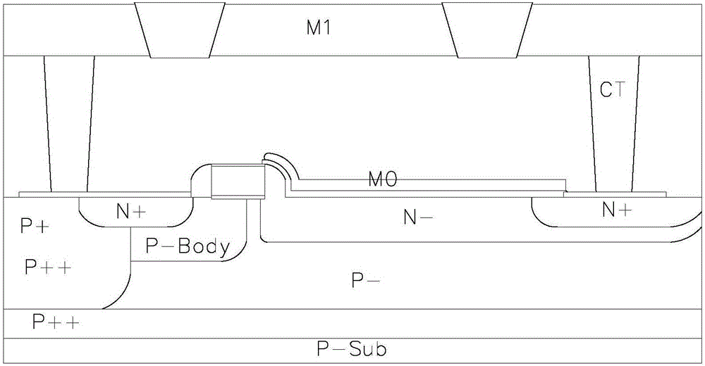
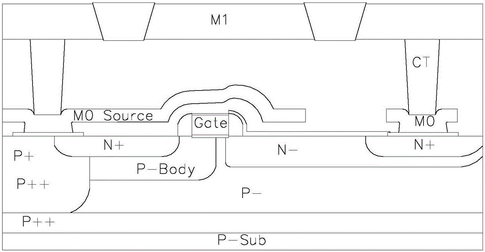
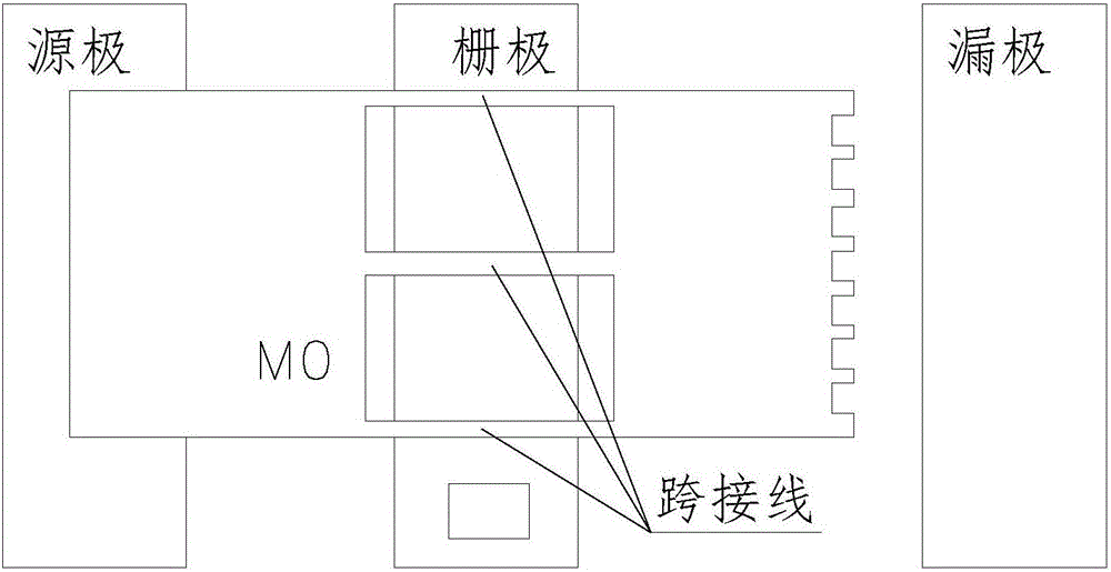
[0034] The present invention resets the layout of the metal shielding layer of the source on the basis of the existing LDMOS structure. join Figure 2 to Figure 7 , the specific structure is as follows:

[0035] The first metal shielding layer M0 of the metal shielding layer spans over the gate, one end of which is connected to the source, and the other end (extended end) extends to the drain but is separated from the drain by a certain distance, so that in the first A coupling capacitance is formed between the metal shielding layer and the oxide or SiN medium of the drain; the thickness of the insulating dielectric layer ILD between the first metal shielding layer and the gate needs to be designed in advance to adjust the size of the coupling capacitance; the metal The distance between the other end of the shielding layer and the gate needs to be designed in advance for adjusting the electric field between the source and drain.

[0036] When necessary, the part of the metal...


PUM


Abstract

The invention provides an LDMOS with low conduction resistance and relatively low total gate charge. The LDMOS comprises a source, a gate, a drain and a metal shielding layer, wherein the metal shielding layer comprises a first metal shielding layer crosses over the upward side of the gate; one end of the first metal shielding layer is positioned below and in contact with the source while a certain distance is formed between the other end of the first metal shielding layer and the drain; the thickness of an insulating dielectric layer between the first metal shielding layer and the gate is used for adjusting the value of a coupling capacitance; and the distance between the other end of the first metal shielding layer and the drain is used for adjusting an electric field between the source and the drain. The technological steps provided by the invention are compatible with a standard CMOS process, an extra mask and a special machine platform are not required; instead, only the ILD thickness and the extension distances of different metal shielding layers M0 need to be adjusted through the process, so that the coupling capacitance is formed between the metal shielding layer and the oxide or silicon nitride SiN and other mediums of the drain; and therefore, different drain electric field coupling is realized, the gate is protected from high voltage impact, and optimization of different voltage devices is realized.

Description

technical field [0001] The invention relates to an LDMOS (Laterally Diffused Metal Oxide Semiconductor) capable of realizing low on-resistance (Ron) and lower total gate charge (Qg) and its preparation process. Background technique [0002] Traditional LDMOS uses an additional mask as a metal shielding layer, such as figure 1 M1 layer in . figure 1 In the M1 layer, metal W, WSi or Ti+TiN is used. [0003] However, since the shielding metal is not compatible with standard CMOS (Complementary Metal Oxide Semiconductor), very few high-speed LDMOSs can provide gate shielding on standard MOS lines. This requires adding an additional mask to reduce the on-resistance and total gate charge, and requires a special machine for implantation. Contents of the invention [0004] The object of the present invention is to provide a LDMOS with low on-resistance and lower total gate charge and its preparation process, which solves the technical problem of high on-resistance and total gat...

Claims


Application Information

Patent Timeline
Patent Type & Authority Applications(China)
IPC IPC(8): H01L29/78H01L21/336H01L23/58H01L21/768
CPCH01L29/7816H01L21/76838H01L23/58H01L23/585H01L29/66681
Inventor 吴杨
Owner 西安阳晓电子科技有限公司
Why Eureka
Eureka Blog
Learn More