

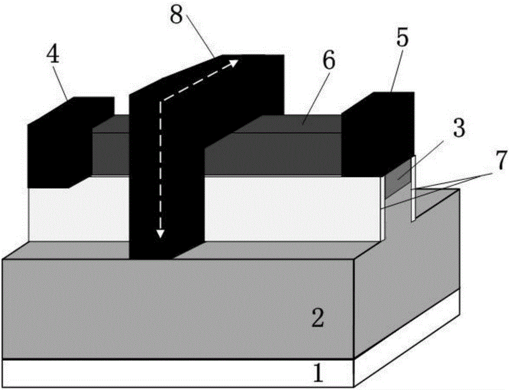
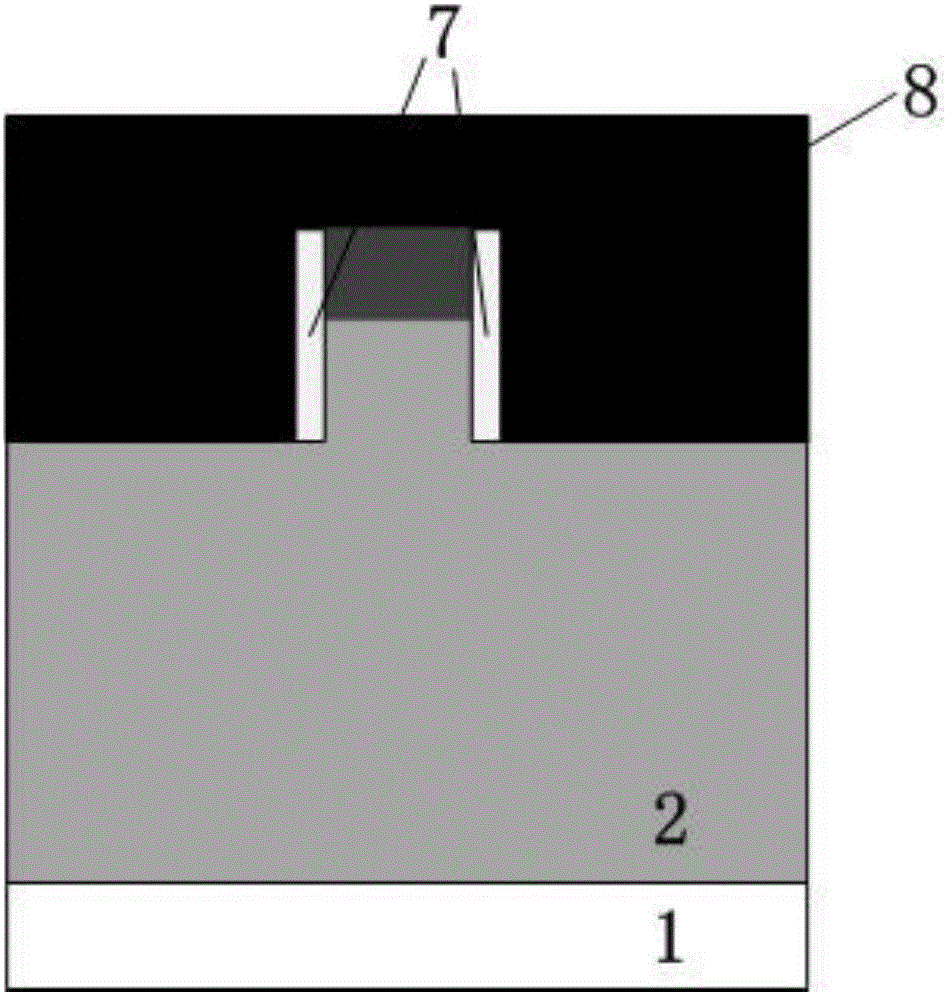
GaN side wall insulated gate fin-type high-electron mobility transistor and manufacturing method thereof
A technology with high electron mobility and manufacturing method, applied in semiconductor/solid-state device manufacturing, circuits, electrical components, etc., can solve the problem that the advantages of FinFET structure are difficult to fully exert, the gate control ability of multi-channel devices is poor, and the gate leakage of FinFET devices increases. Large and other problems, to achieve the effect of solving the degradation of the maximum operating gate voltage, increasing the maximum operating frequency, and increasing the maximum driving current
- Summary
- Abstract
- Description
- Claims
- Application Information
AI Technical Summary
Problems solved by technology
Method used
Image

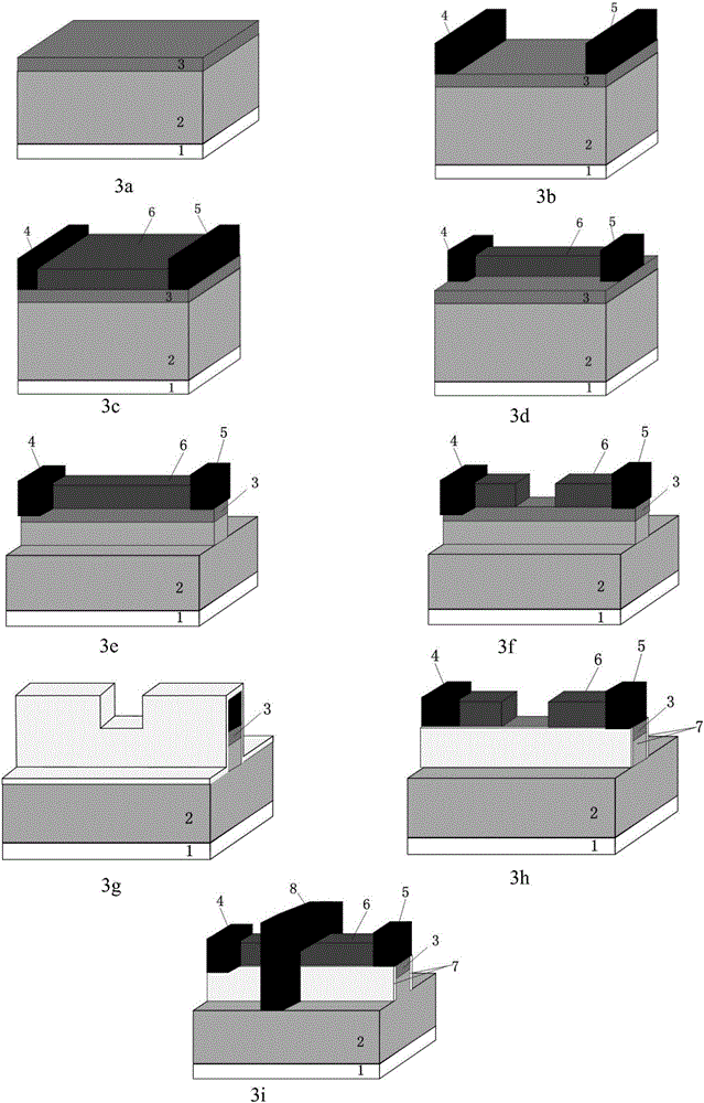
Examples
Embodiment 1
[0046] Example 1: Prepare a SiC substrate, the buffer layer is AlN / GaN, the barrier layer is AlGaN, the sidewall dielectric is SiN, the three-dimensional fin width is 120nm, and the gate metal is Pt / Au GaN sidewall insulating gate fin type height Electron mobility transistor, the process is:
[0047] 1) On the SiC substrate, using metal organic chemical vapor deposition technology MOCVD, first grow 200nm AlN at 1050°C, and then grow a 1.5μm unintentionally doped GaN layer at 1050°C to form a buffer layer 2, Subsequently, an AlGaN barrier layer 3 with a thickness of 28 nm is grown on the buffer layer 2 with an Al composition of 25%.
[0048] 2) Make a photolithographic mask on the barrier layer 3, and then use sputtering to deposit metal stacks, and obtain isolated metal blocks at both ends through a lift-off process, and finally place them on the N 2 Rapid thermal annealing is performed in the atmosphere to form the source 4 and the drain 5 . The deposited metals are Ti, Al,...
Embodiment 2
[0058] Example 2: Prepare Si substrate, the buffer layer is AlGaN / GaN, the barrier layer is AlN, and the side wall dielectric is Al 2 o 3 , the three-dimensional fin width is 300nm, the gate metal is Ni / Pt / Au GaN sidewall insulated gate fin type high electron mobility transistor, the process is:
[0059] 1) On the SiC substrate, a 1.0 μm non-intentionally doped AlGaN layer (Al composition 5%) and a 1.0 μm GaN layer were grown at 1000 ° C by metal organic chemical vapor deposition technology MOCVD to form a buffer layer 2, and then grow an AlN barrier layer 3 with a thickness of 3 nm on the buffer layer 2.
[0060] 2) Make a photolithographic mask on the barrier layer 3, then use electron beam evaporation to deposit a metal stack, and obtain isolated metal blocks at both ends through a lift-off process, and finally in N 2 Rapid thermal annealing is performed in the atmosphere to form the source 4 and the drain 5 . The deposited metals are Ti, Al, Mo and Au from bottom to top...
PUM
 Abstract
Description
Claims
Application Information