

Method for assisting high-temperature laser brazing through self-propagating reaction of nano-multilayer film
A nano-multilayer, laser-assisted technology, applied in welding equipment, welding equipment, manufacturing tools, etc., to achieve the effect of reducing requirements, reducing heat-affected zone, and increasing joint area
- Summary
- Abstract
- Description
- Claims
- Application Information
AI Technical Summary
Problems solved by technology
Method used
Image

Examples
Embodiment 1
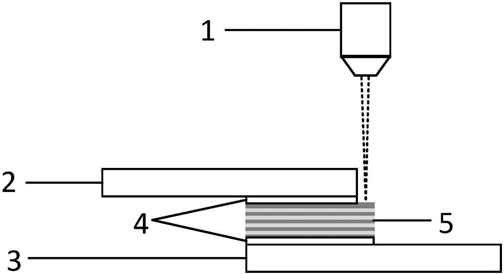
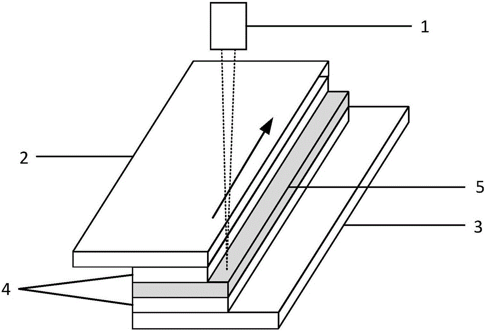
[0032] 1) The silicon substrate was ultrasonically cleaned in alcohol and pure water for 5 min, respectively. Wash and dry.
[0033] 2) Magnetron sputtering is used to deposit nanometer multilayer films of Ti and Ni on the substrate. The process parameters of magnetron sputtering deposition: the deposition power is 250W, the Ar gas flow is 40sccm, the working pressure is 0.5Pa, and the background vacuum is 5*10 -4 Pa. The deposition time of Ti is 60s and that of Ni is 45s. Alternate deposition for 400 cycles. The thickness of the obtained multilayer film was about 24 μm.
[0034] 3) The deposited multilayer film is peeled off from the silicon substrate.
[0035] 4) The peeled multilayer film is placed between two layers of 30 μm thick SnAgCu solder foil to form a composite intermediate layer.
[0036] 5) Surface pretreatment of the base metal to be welded, using #200 sandpaper, #400 sandpaper, #600 sandpaper, #800 sandpaper and #1000 sandpaper to polish layer by layer un...
Embodiment 2
[0042] The difference between this embodiment and the first embodiment is that the magnetron sputtering is used to deposit the nanometer multilayer film of Ti and Al in the second step. The process parameters of magnetron sputtering deposition: the deposition power is 200W, the deposition time of Ti is 70s, the deposition time of Al is 40s, the deposition cycle is 300 cycles, and the thickness of the obtained multilayer film is about 20 μm. Others are the same as in Embodiment 1.
Embodiment 3
[0044] The difference between this embodiment and the first or second embodiment is that the nanometer multilayer film of Ni and Al is deposited by magnetron sputtering as described in the second step. The process parameters of magnetron sputtering deposition: the deposition power is 300W, the deposition time of Ni is 60s, the deposition time of Al is 50s, and the alternate deposition is 400 cycles, and the thickness of the obtained multilayer film is about 28 μm. Others are identical with embodiment one or two.
PUM
| Property | Measurement | Unit |
|---|---|---|
| Thickness | aaaaa | aaaaa |
| Thickness | aaaaa | aaaaa |
Abstract
Description
Claims
Application Information