Gan-based lasers and superluminescent light-emitting diodes and manufacturing methods thereof

A superluminescence and laser technology, applied in lasers, laser components, semiconductor lasers, etc., can solve problems such as reduced current injection efficiency, device performance deterioration, and weakened lateral confinement, so as to improve device reliability and avoid etching damage , The effect of reducing the threshold current

Active Publication Date: 2019-07-05
SUZHOU INST OF NANO TECH & NANO BIONICS CHINESE ACEDEMY OF SCI
View PDF7 Cites 0 Cited by
  • Summary
  • Abstract
  • Description
  • Claims
  • Application Information

AI Technical Summary

Problems solved by technology

Since dry etching usually introduces surface states and defects, these surface states and defects will become leakage channels, affecting the reliability and stability of the device
In order to reduce the impact of etching damage, a dielectric film is usually deposited at the etching site to passivate the surface states and defects. However, the lattice mismatch and thermal mismatch between the dielectric film and the nitride are usually large, and the etching cannot be completely passivated. damage
In order to reduce the impact of etching damage, conventional lasers and superluminescent light-emitting diodes basically use shallow etching, usually only etching to the upper confinement layer, but etching damage will still affect the characteristics of the laser
[0004] Since lasers and superluminescent light-emitting diodes are etched only to the upper confinement layer by shallow etching, the remaining upper confinement layer, upper waveguide layer and quantum well will become optical waveguides, causing the light field to leak, resulting in weakened lateral confinement. As a result, the lateral divergence angle of the laser and superluminescent light-emitting diode spots is small, the aspect ratio is large, and it is elliptical, which affects the coupling of the spot, etc.
[0005] Also, the upper confinement layer of lasers and superluminescent light-emitting diodes is usually an AlGaN / GaN superlattice structure. Due to polarization effects, there are two-dimensional hole gases in GaN at the interface of the superlattice, resulting in a relatively low lateral transmission resistance of the superlattice. Small, much smaller than its longitudinal transmission resistance, so the upper confinement layer that has not been etched completely will act as a current expansion channel, and the holes injected from the ridge are easy to expand laterally here, extending to the current and light field beyond the ridge Miscoincidence, unable to generate gain, no help to laser lasing, equivalent to leakage current, resulting in reduced current injection efficiency, increased threshold current of lasers and superluminescent light-emitting diodes, and degraded device performance
[0006] In addition, the functional layers in lasers and superluminescent light-emitting diodes are uniformly and continuously grown on heterogeneous substrates. As the size of the substrate increases, the stress in lasers and superluminescent light-emitting diodes gradually increases, which easily leads to excessive warping of epitaxial wafers. , which is not conducive to the subsequent device manufacturing process and affects the device yield; when the stress is large enough, cracks will occur in the epitaxial wafer, which seriously affects the device performance and yield

Method used


Image

  • Gan-based lasers and superluminescent light-emitting diodes and manufacturing methods thereof
  • Gan-based lasers and superluminescent light-emitting diodes and manufacturing methods thereof
  • Gan-based lasers and superluminescent light-emitting diodes and manufacturing methods thereof

Examples


Embodiment 1

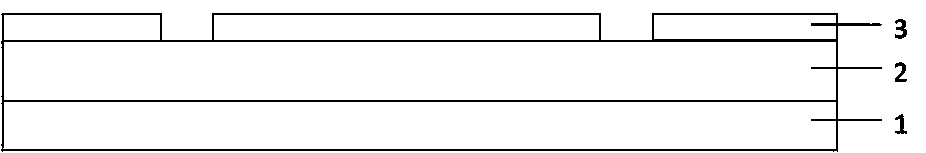
[0051] Embodiment 1 The GaN-based blue laser and superluminescent light-emitting diode structure of this embodiment can refer to Figure 4 , which can be grown and formed by the selective area epitaxy method, which specifically includes the following steps:

[0052] S1: Put the substrate into MOCVD, raise the temperature to about 1080°C, and pretreat the substrate at high temperature for about 5 minutes in a hydrogen atmosphere to remove impurities on the surface of the substrate, and then inject a small amount of NH 3 Nitriding the substrate surface;

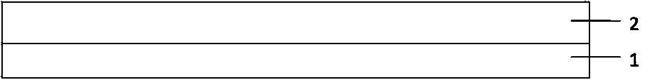
[0053] S2: Cool down to about 530°C, grow a GaN nucleation layer of about 25nm, perform high temperature (about 1000°C) annealing on the GaN nucleation layer, and grow an undoped GaN layer of about 1 μm and n-GaN of about 2 μm at high temperature layer, such as figure 1 shown;

[0054] S3: After the growth is over, take out the epitaxial wafer, and deposit about 200nm of SiO on the surface of the sample by plasma enhanced ch...

Embodiment 2

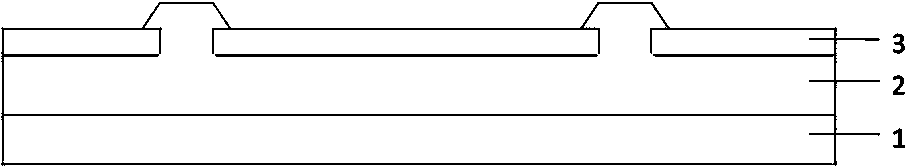
[0061] Embodiment 2 The GaN-based blue laser and the superluminescent light-emitting diode of this embodiment can be based on Figure 5 The growth and formation of the substrate shown specifically includes the following steps:

[0062] S1: Put the substrate into MOCVD, raise the temperature to about 1080°C, and pretreat the substrate at high temperature for about 5 minutes in a hydrogen atmosphere to remove impurities on the surface of the substrate, and then inject a small amount of NH 3 Nitriding the substrate surface;

[0063] S2: Cool down to about 530°C, grow a GaN nucleation layer of about 25nm, perform high temperature (about 1000°C) annealing on the GaN nucleation layer, and grow an undoped GaN layer of about 1 μm and n-GaN of about 2 μm at high temperature layer, such as figure 1 shown;

[0064] S3: After the growth is over, take out the epitaxial wafer, and deposit about 200nm of SiO on the surface of the sample by plasma enhanced chemical vapor deposition (PECVD)...


PUM


Abstract

The invention discloses a GaN-based laser, a superluminescent light-emitting diode and a preparation method thereof. The ridge structure of the laser and the superluminescent light-emitting diode is directly formed by epitaxial growth, which includes a substrate with a strip-shaped step structure distributed on the surface, and is arranged on the substrate and covers the strip-shaped step structure. An epitaxial layer with a ridge structure, the epitaxial layer comprising a lower contact layer, a lower confinement layer, a lower waveguide layer, an active layer, an upper waveguide layer, an electron blocking layer, an upper confinement layer and an upper contact layer formed sequentially on the substrate . In the present invention, by forming a window area on the substrate or pre-etching to form a stepped structure, the laser and the superluminescent light-emitting diode ridge are directly grown on the substrate, and optical confinement layers are grown on both sides of the ridge structure, which can not only effectively The lateral limitation of the device is improved, the threshold current of the device is reduced, and the etching operation can be omitted at the same time, so as to avoid etching damage, further reduce the threshold current of the device, and improve the reliability of the device.

Description

technical field [0001] The invention relates to a semiconductor laser, a superluminescent light-emitting diode and a preparation method thereof, in particular to a GaN-based laser with a ridge waveguide structure, a superluminescent light-emitting diode and a preparation method thereof, belonging to the field of semiconductor photoelectric technology. Background technique [0002] III-V nitride semiconductors are called third-generation semiconductor materials, which have the advantages of large band gap, good chemical stability, and strong radiation resistance; their band gap covers the entire visible light range, so they can be used to make semiconductor light-emitting Devices such as light-emitting diodes, lasers, and superluminescent light-emitting diodes. Lasers and superluminescent light-emitting diodes based on III-V nitride semiconductors have the advantages of simple fabrication, small size, light weight, long life, and high efficiency, and have been widely used in ...

Claims


Application Information

Patent Timeline
Patent Type & Authority Patents(China)
IPC IPC(8): H01S5/343
Inventor 孙钱冯美鑫周宇杨辉池田昌夫刘建平张书明李德尧张立群
Owner SUZHOU INST OF NANO TECH & NANO BIONICS CHINESE ACEDEMY OF SCI
Why Eureka
Try Eureka