Controlled synthesis method for PbI2 micro-nano structure
A synthesis method and micro-nano structure technology, applied in the direction of nanotechnology, nanotechnology, nanotechnology for materials and surface science, etc., to achieve the effects of low energy consumption, simple operation, and low equipment requirements
- Summary
- Abstract
- Description
- Claims
- Application Information
AI Technical Summary
Problems solved by technology
Method used
Image

Examples
Embodiment 1
[0025] a PbI 2 The control synthesis method of micro-nano structure, its specific method is:
[0026] a. Prepare the solution
[0027] At 25°C, weigh 0.10 g of PbI 2 powder, it was completely dissolved in 15mL of tetrahydrofuran, and stirred;
[0028] b. Sonication and Stirring
[0029] The solution was sonicated for 10 minutes, then stirred for an additional 3 hours, and allowed to stand;
[0030] c. Isolation and Preparation
[0031] After standing still for 24 hours, separate the upper layer solution and the lower layer precipitation, and use a dropper to take an appropriate solution on a clean silicon chip, and obtain PbI after drying. 2 nanosheets; at the same time, the lower precipitate was filtered and dried to obtain PbI 2 Micron wire.
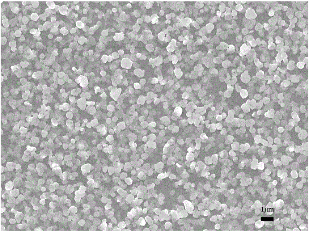
[0032] figure 1 It is the PbI obtained in Example 1 of the present invention 2 Scanned photographs (SEM) of the nanosheets, from figure 1 It can be seen that the obtained product has a sheet-like structure with a width of abo...
Embodiment 2
[0042] a PbI 2 The control synthesis method of micro-nano structure, its specific method is:
[0043] a. Prepare the solution
[0044] At 25°C, weigh 0.15g of PbI 2 powder, completely dissolve it in 20mL of tetrahydrofuran, and stir;
[0045] b. Sonication and Stirring
[0046] The solution was sonicated for 10 minutes, then continued to stir for 3 hours, and then allowed to stand;
[0047] c. Isolation and Preparation
[0048] After standing still for 24 hours, separate the upper layer solution and the lower layer precipitation, and use a dropper to take an appropriate solution on a clean silicon chip, and obtain PbI after drying. 2 nanosheets; at the same time, the lower precipitate was filtered and dried to obtain PbI 2 Micron wire.
[0049] Figure 3a It is the PbI obtained in Example 2 of the present invention 2 Scanned photographs (SEM) of the nanosheets, from Figure 3aIt can be seen that the obtained product has a sheet-like structure with a width of 300-500 ...
Embodiment 3
[0060] a PbI 2 The control synthesis method of micro-nano structure, its specific method is:
[0061] a. Prepare the solution
[0062] At 25°C, weigh 0.13g of PbI 2 powder, it was completely dissolved in 15mL of tetrahydrofuran, and stirred;
[0063] b. Sonication and Stirring
[0064] The solution was sonicated for 10 minutes, then stirred for an additional 3 hours, and allowed to stand;
[0065] c. Isolation and Preparation
[0066] After standing still for 24 hours, separate the upper layer solution and the lower layer precipitation, and use a dropper to take an appropriate solution on a clean silicon chip, and obtain PbI after drying. 2 nanosheets; at the same time, the lower precipitate was filtered and dried to obtain PbI 2 Micron wire.
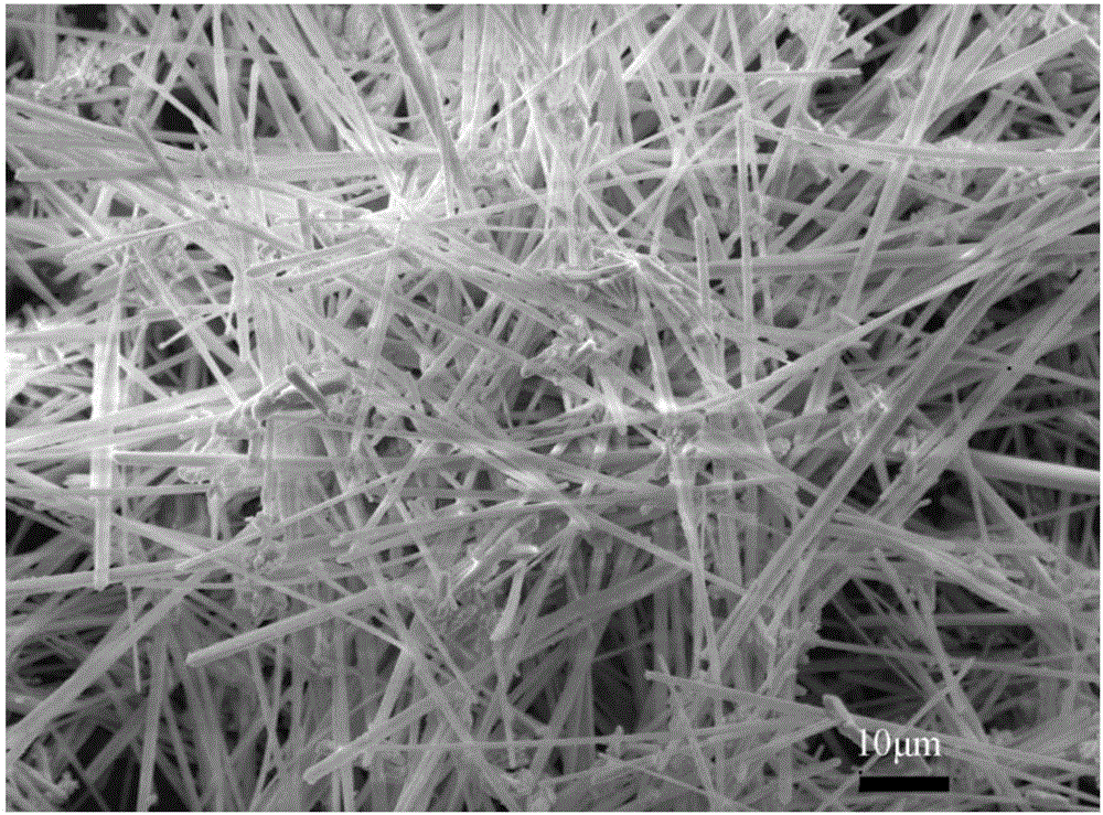
[0067] Figure 5a Be the PbI that the embodiment of the present invention three obtains The scanning photo (SEM) of nanosheet, by Figure 5a It can be seen that the product is a nanosheet with a wide size distribution, ranging ...
PUM
 Abstract
Description
Claims
Application Information
 - R&D
- Intellectual Property
- Life Sciences
- Materials
- Tech Scout
- Unparalleled Data Quality
- Higher Quality Content
- 60% Fewer Hallucinations
Browse by: Latest US Patents, China's latest patents, Technical Efficacy Thesaurus, Application Domain, Technology Topic, Popular Technical Reports.
© 2025 PatSnap. All rights reserved.Legal|Privacy policy|Modern Slavery Act Transparency Statement|Sitemap|About US| Contact US: help@patsnap.com