Wide-band-gap naphthalene organic semiconductor materials as well as preparation method and application thereof

An organic semiconductor and wide-bandgap technology, which is applied in the field of wide-bandgap naphthalene-based organic semiconductor materials and its preparation, can solve the problems of increased cost and instability of vacuum and light-shielding technologies, and achieve good thermal stability and light stability with low cost , the effect of high yield

Active Publication Date: 2017-06-13
NANJING UNIV OF TECH
View PDF9 Cites 0 Cited by
  • Summary
  • Abstract
  • Description
  • Claims
  • Application Information

AI Technical Summary

Problems solved by technology

In the acene series, pentacene and rubrene both exhibit high hole mobility, but they are extremely unstable in air, and vacuum and light-shielding technologies have greatly increased the cost

Method used

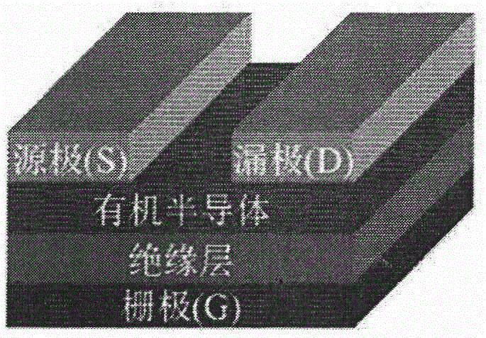
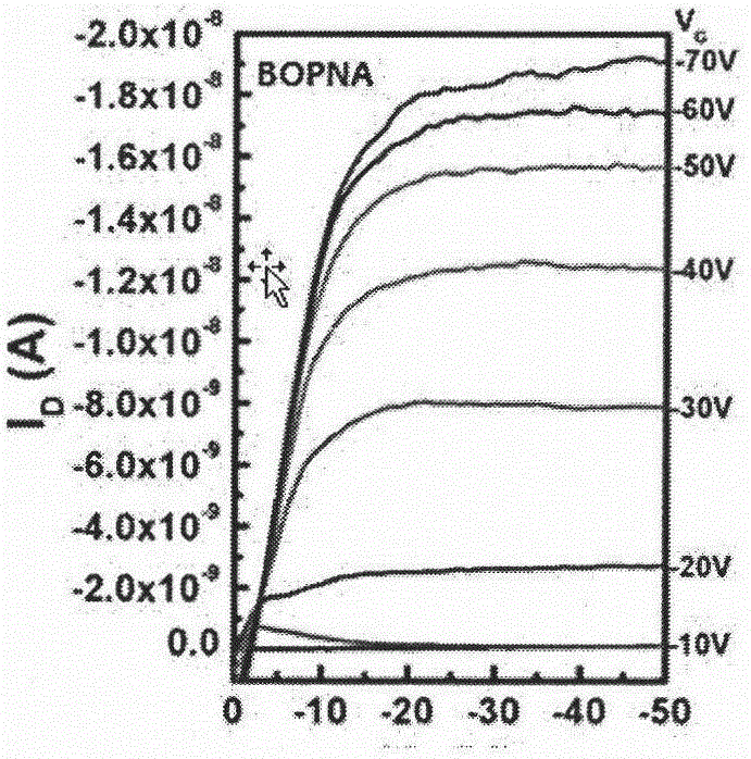
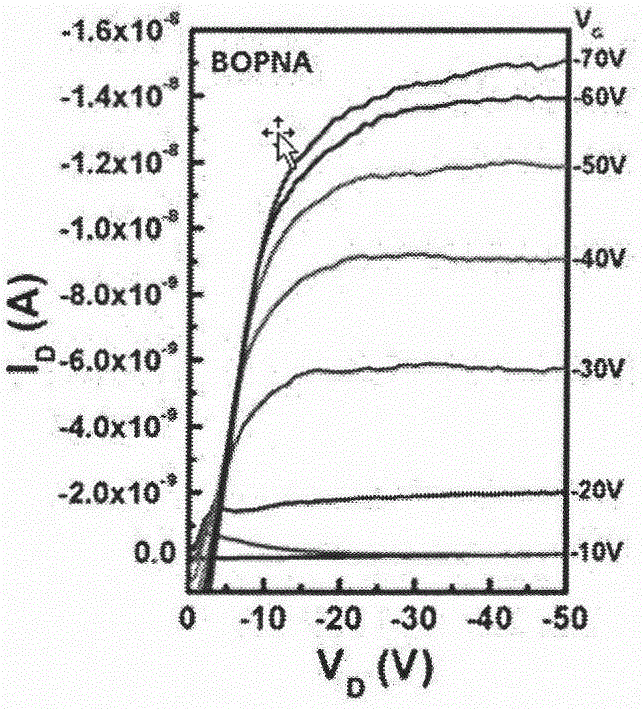

Image

  • Wide-band-gap naphthalene organic semiconductor materials as well as preparation method and application thereof
  • Wide-band-gap naphthalene organic semiconductor materials as well as preparation method and application thereof
  • Wide-band-gap naphthalene organic semiconductor materials as well as preparation method and application thereof

Examples


Embodiment 1

[0024] A wide bandgap naphthalene organic semiconductor material 2,6-bis(4-methoxybenzene)naphthalene (named BOPNA), its structural formula is:

[0025]

[0026] The preparation method of above-mentioned organic semiconductor material BOPNA comprises the steps:

[0027]

[0028] Into the reaction vessel, 2,6-dibromonaphthalene (5.76g, 20mmol), 4-methoxyphenylboronic acid (9.18g, 60mmol) and 150ml of toluene were successively added and mixed uniformly. Add saturated aqueous sodium carbonate solution (60ml) and tetrakistriphenylphosphopalladium (0.46g, 0.4mmol), pass nitrogen gas into the reaction solution for 20 minutes, heat the reaction solution to 105°C, reflux for 24 hours, turn off the heating, Stop responding. The obtained reaction solution was washed with methanol, dilute hydrochloric acid solution, and acetone successively, and 6.11 g (yield: 90%) of a white crude product was obtained after filtration. After the crude product was purified three times in a vacuum ...

Embodiment 2

[0030] A wide bandgap naphthalene organic semiconductor material 2,6-bis(4-methylthiophenyl)naphthalene (named BSPNA), its structural formula is:

[0031]

[0032] The preparation method of above-mentioned organic semiconductor material BSPNA, comprises the steps:

[0033] Into the reaction vessel, add 2,6-dibromonaphthalene (5.76g, 20mmol), 4-methylthiophenylboronic acid (10.08g, 60mmol) and 150ml of toluene in sequence, and mix well. Add saturated aqueous sodium carbonate solution (60ml) and tetrakistriphenylphosphopalladium (0.46g, 0.4mmol), pass nitrogen gas into the reaction solution for 20 minutes, heat the reaction solution to 105°C, reflux for 24 hours, turn off the heating, Stop responding. The obtained reaction solution was washed with methanol, dilute hydrochloric acid solution and acetone successively, and 6.53 g (yield 88%) of a white crude product was obtained after filtration. After the crude product was purified three times in a vacuum tube furnace, a light...

Embodiment 3

[0035] A wide bandgap naphthalene organic semiconductor material 2,6-bis(4-ethylbenzene)naphthalene (named BCPNA), its structural formula is:

[0036]

[0037] The preparation method of above-mentioned organic semiconductor material BCPNA, comprises the steps:

[0038] Into the reaction vessel, 2,6-dibromonaphthalene (5.76g, 20mmol), 4-ethylphenylboronic acid (9.00g, 60mmol) and 150ml of toluene were successively added and mixed uniformly. Add saturated aqueous sodium carbonate solution (60ml) and tetrakistriphenylphosphopalladium (0.46g, 0.4mmol), pass nitrogen gas into the reaction solution for 20 minutes, heat the reaction solution to 105°C, reflux for 24 hours, turn off the heating, Stop responding. The obtained reaction solution was washed with methanol, dilute hydrochloric acid solution, and acetone successively, and 6.18 g (92% yield) of a white crude product was obtained after filtration. The crude product was purified three times in a vacuum tube furnace to obtain a...


PUM

PropertyMeasurementUnit
Hole mobilityaaaaaaaaaa

Abstract

The invention relates to wide-band-gap naphthalene organic semiconductor materials as well as a preparation method and an application thereof. The general structural formula of the wide-band-gap organic semiconductor materials is shown in the specification. The compounds adopting the structure have wider band gaps, better heat stability and light stability and excellent carrier transport efficiency, can be widely applied to optical devices such as organic light-emitting devices, organic field effect transistor devices and the like and has the advantages of good universality and repeatability and the like; a synthesis route is simple and efficient, raw materials are cheap, synthesis cost is low, and the synthesis route is applicable to industrial production.

Description

technical field [0001] The invention relates to the field of optoelectronic materials, in particular to a class of wide-bandgap naphthalene organic semiconductor materials and a preparation method and application thereof. Background technique [0002] With the rapid development of electronic technology, organic field effect transistors can be widely used in large-area flexible displays, smart cards, sensors and radio frequency tags due to their low cost, simple preparation process, compatibility with flexible biological substrates, and chemical modification. and other fields. With the development of modern electronic equipment, the need for transparent electronic equipment is becoming more and more extensive, and transparent thin film transistors have become a research hotspot for scientific researchers. So far, most of the semiconductor materials used in transparent transistors are inorganic oxide semiconductor materials, such as zinc oxide (ZnO), tin oxide (SnO x ), indi...

Claims


Application Information

Patent Timeline
IPC IPC(8): C07C41/30C07C43/205C07C319/20C07C321/28C07C1/32C07C15/24C09K11/06H01L51/54H01L51/05H01L51/30
CPCC09K11/06C07C1/321C07C15/24C07C41/30C07C43/205C07C319/20C07C321/28C09K2211/1011H10K85/615
Inventor 孟鸿闫丽佳赵亮黄维
Owner NANJING UNIV OF TECH
Why Eureka
Try Eureka