Gallium nitride PN junction realized by injecting fluorine ions and manufacturing method of gallium nitride PN junction

A manufacturing method and technology of fluoride ions, which are applied in semiconductor/solid-state device manufacturing, electrical components, diodes, etc., can solve difficult problems, and achieve low cost, precise and controllable concentration and depth distribution, and high doping uniformity. Effect

Inactive Publication Date: 2017-06-13
JIANGNAN UNIV
View PDF3 Cites 4 Cited by
  • Summary
  • Abstract
  • Description
  • Claims
  • Application Information

AI Technical Summary

Problems solved by technology

The unintentional doping type of in-situ grown GaN is n-type, which has a high background carrier concentration. The n-type background carrier will have a strong compensation effect on the p-type, so the p-type doping of GaN is relatively It is more difficult for n-type

Method used


Image

  • Gallium nitride PN junction realized by injecting fluorine ions and manufacturing method of gallium nitride PN junction
  • Gallium nitride PN junction realized by injecting fluorine ions and manufacturing method of gallium nitride PN junction
  • Gallium nitride PN junction realized by injecting fluorine ions and manufacturing method of gallium nitride PN junction

Examples


Embodiment Construction

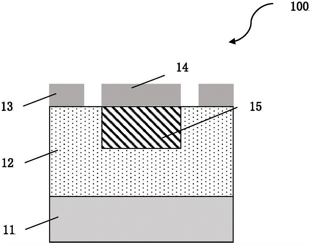
[0040] The drawings in the present invention are all schematic diagrams, mainly intended to represent the manufacturing process steps and the upper-lower sequence relationship between each layer, and the shapes, thicknesses and widths are not drawn to scale.

[0041] figure 1 An embodiment of the invention is shown. This embodiment illustrates a schematic cross-sectional view of a manufacturing method of a GaN-based PN junction 100 realized by fluorine ion implantation. First, a substrate 11 is provided, such as but not limited to a silicon (silicon, Si) substrate, a sapphire substrate, or an unintentionally doped gallium nitride (gallium nitride, GaN) substrate. On the substrate 11 , an n-type GaN semiconductor layer 12 is grown by, for example but not limited to, epitaxial technology. Next, fluorine ions are implanted into the middle region of the n-type GaN semiconductor layer 12 by ion implantation technology to form the p-type GaN semiconductor layer 15 . Wherein, the ...


PUM


Abstract

The invention discloses a gallium nitride PN junction realized by injecting fluorine ions and a manufacturing method of the gallium nitride PN junction. The gallium nitride PN junction comprises a substrate, an n-type gallium nitride semiconductor layer disposed on the substrate and a p-type gallium nitride semiconductor layer embedded in a middle area of the n-type gallium nitride semiconductor layer. An n-type doping gallium nitride semiconductor layer is provided with a first electrode, and a p-type doping gallium nitride semiconductor layer is provided with a second electrode. The preparation method for realizing the gallium nitride-based PN junction by injecting the fluorine ions is compatible with the existing silicon process, the distribution of the concentration and depth of the injected fluorine ions is precisely controllable, and the formed p-type gallium nitride semiconductor layer has high doping uniformity. The preparation process is simple, and the cost is low.

Description

technical field [0001] The present invention relates to the technical field of semiconductors, in particular to a PN junction based on gallium nitride (GaN) material and a manufacturing method thereof. Background technique [0002] Currently, the growth methods of GaN-based PN junctions are mostly based on metal organic chemical vapor deposition (metal organic chemical vapor deposition, MOCVD) method. The unintentional doping type of in-situ grown GaN is n-type, which has a high background carrier concentration. The n-type background carrier will have a strong compensation effect on the p-type, so the p-type doping of GaN is relatively It is more difficult for n-type. The existing method of forming a p-type doped GaN semiconductor layer is to irradiate the in-situ grown Mg-doped GaN with low-energy electrons or anneal at a high temperature in a nitrogen atmosphere to obtain effectively doped p-type GaN. [0003] The silicon (silicon, Si) process generally adopts ion implan...

Claims


Application Information

Patent Timeline
Patent Type & Authority Applications(China)
IPC IPC(8): H01L29/861H01L21/265H01L21/266H01L21/329
CPCH01L29/66204H01L29/8613H01L21/2654H01L21/266
Inventor 赵琳娜闫大为顾晓峰陈雷雷
Owner JIANGNAN UNIV
Why Eureka
Try Eureka