Printed circuit board pcb and its non-destructive testing method and device

A printed circuit board, non-destructive testing technology, used in printed circuit components, circuit inspection/identification, etc., can solve problems such as tight PCB layout area, signal quality degradation, signal distortion, etc., to save layout area and reduce test costs. , the effect of eliminating signal distortion

Inactive Publication Date: 2019-06-07
QIKU INTERNET TECH SHENZHEN CO LTD
View PDF3 Cites 0 Cited by
  • Summary
  • Abstract
  • Description
  • Claims
  • Application Information

AI Technical Summary

Problems solved by technology

[0007] 1. Nowadays, the circuits of smart electronic consumer products are complex, the PCB layout area is very tight, and the test points generally have a large area
It will take up valuable layout area on the PCB, and as the number of signals to be tested increases, it is unrealistic to add test points for each signal
[0008] 2. If the test point itself is not on the PCB trace signal, the test signal needs to pull a section of trace to the test point, thereby introducing the stub effect. For high-speed signals, it will cause signal reflection, distortion, and cause signal The decline in quality, or even cause the system not to work
[0009] 3. If the test point itself is on the PCB trace signal, the diameter of the test point is much wider than the trace, which will cause a sudden change in the impedance of the trace, and the parasitic capacitance of the test point itself is also large, which will cause signal reflection, ringing and other distortions. Cause the signal quality to drop, even cause the system not to work
[0010] 4. Increase PCB cost, because the surface treatment process of test points generally requires gold plating treatment, too many test points will lead to an increase in PCB cost, thereby increasing the cost of the whole machine
[0012] 1. When the engineer scrapes off the surface of the PCB with a scraper or other mechanical methods, the position of the tested line cannot be accurately determined because the line is covered by the solder mask.
[0013] 2. It is easy to scratch and break the circuit, resulting in the scrapping of the PCB as a whole
[0014] 3. When scraping off the solder mask, the line under test is easily scraped thin, and the change in the thickness of the PCB line will affect the DC resistance and characteristic impedance of the line.
The solder mask on the line is scraped off, and the environment of the PCB trace changes, which will also lead to a change in the characteristic impedance of the trace; these will cause signal distortion, cause a decrease in signal quality, and even cause the system to fail to work
[0015] 4. It is a destructive test. After the test is completed, the appearance of the PCB is severely damaged, and it cannot be shipped as a normal product, resulting in an increase in the cost of the entire product project.

Method used


Image

  • Printed circuit board pcb and its non-destructive testing method and device
  • Printed circuit board pcb and its non-destructive testing method and device
  • Printed circuit board pcb and its non-destructive testing method and device

Examples


Embodiment 1

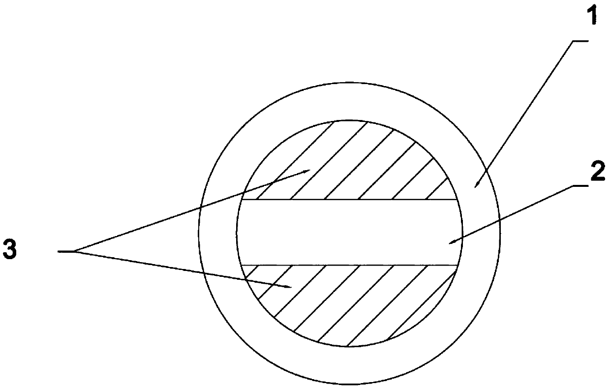
[0060] refer to figure 1 and figure 2 , the present invention proposes a printed circuit board (PCB). The solder resist on the surface of the PCB is solder resist cured by solvent-based ink. The position of the circuit 2 to be tested on the solder resist surface is provided with a raised silk screen ring 1, and the silk screen ring 1 is a non-solvent The silk screen ring 1 formed by solidifying ink, the inner circle of the silk screen ring 1 corresponds to the line 2 to be tested and the forbidden areas 3 distributed on both sides of the line 2 to be tested.

[0061] During PCB processing, the PCB is processed and produced according to the conventional PCB process, and the solder mask on the surface of the PCB is processed with solvent-based ink. After the solder mask is cured, the silk screen ring 1 on the surface of the PCB is processed with non-solvent ink. In the way of printing, since the ink of the silk screen ring 1 is printed on the upper layer of the cured solder ma...

Embodiment 2

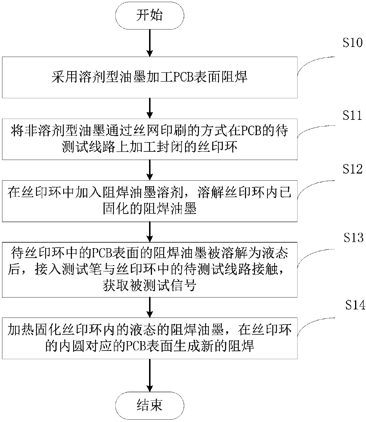
[0065] refer to image 3 , the present invention also proposes a method for non-destructive testing of the printed circuit board PCB as described in Embodiment 1, comprising the following steps:

[0066] S10, using solvent-based ink to process the solder mask on the surface of the PCB.

[0067] S11. Process a closed silk-screen ring on the circuit 2 to be tested on the PCB by screen-printing non-solvent ink.

[0068] S12 , adding a solder resist ink solvent into the silk screen printing ring 1 to dissolve the cured solder resist ink in the silk screen printing ring 1 .

[0069] S13. After the solder resist ink on the surface of the PCB in the silk screen ring 1 is dissolved into a liquid state, a test pen is connected to contact the circuit 2 to be tested in the silk screen ring 1 to obtain a signal to be tested.

[0070] S14 , heat and solidify the liquid solder resist ink in the silk screen ring 1 , and generate new solder resist on the surface of the PCB corresponding to ...

Embodiment 3

[0094] refer to Figure 5 , the present invention also proposes a device for non-destructive testing of the printed circuit board PCB described in Embodiment 1, including:

[0095] The solder resist processing unit 10 is used for processing the solder resist on the surface of the PCB with solvent-based ink.

[0096] The silk screen ring processing unit 20 is used to process the closed silk screen ring 1 on the circuit 2 to be tested on the PCB by screen printing with non-solvent ink.

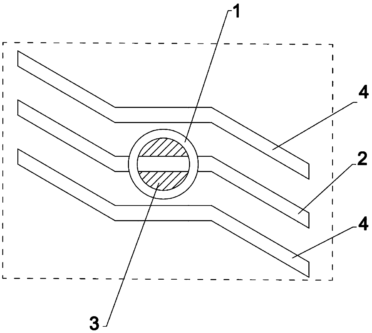
[0097]A marking unit 30 is provided for setting a signal marking silk screen around the silk screen ring 1 for identifying the circuit 2 to be tested.

[0098] The positioning unit 40 is used to determine the position of the silk screen ring 1 according to the signal mark silk screen, and determine the specific position of the corresponding circuit 2 to be tested.

[0099] The dissolving unit 50 is used to add a solder resist ink solvent into the silk screen printing ring 1 to dissolve the cur...


PUM


Abstract

The present invention discloses a printed circuit board (PCB) and a method and device of a lossless test thereof. The surface solder resist of the PCB is a solder resist formed by solvent-based ink solidification, a raised silk-screen ring is arranged at the position of a line to be tested at the surface solder resist, the silk-screen ring is formed by the non-solvent based ink solidification, and the inner circle of the silk-screen ring corresponds to the line to be tested and arrangement prohibit zones distributed at two sides of the line to be tested. The method comprises the following steps: adding a solder resist ink solvent in the silk-screen ring, and dissolving the solidified solder resist ink in the silk-screen ring; contacting an access test pen with the line to be tested in the silk-screen ring after the solder resist ink at the PCB surface in the silk-screen ring is dissolved to liquid state, and obtaining signals to be tested. Compared to test points generally employed in the prior art, the printed circuit board (PCB) and the method and device of the lossless test thereof can greatly reduce occupation area of test points, avoid PCB appearance damaging caused by striking off surface solder resist by using a scraper blade, and circularly perform repeat test without PCB appearance damaging.

Description

technical field [0001] The invention relates to the field of PCB signal testing, in particular to a PCB and a non-destructive testing method and device thereof. Background technique [0002] With the rapid development and popularization of smart electronic consumer products, and the development of smart electronic products towards thinner and higher density, the layout density of components in smart electronic consumer products, especially smart phone products, is also increasing. PCB (Printed Circuit Board , printed circuit board) wiring is becoming more and more dense, and the signal rate of the line on the PCB is getting higher and higher. This leads to the need to test numerous signals during the hardware testing phase. [0003] The existing PCB hardware signal testing methods mainly adopt the following two methods: [0004] A. During PCB design, reserve test points on the circuit that needs to be tested in the later stage. During the later test, touch the test point w...

Claims


Application Information

Patent Timeline
Patent Type & Authority Patents(China)
IPC IPC(8): H05K1/02
CPCH05K1/0268
Inventor 李帅
Owner QIKU INTERNET TECH SHENZHEN CO LTD
Why Eureka
Try Eureka