

Plasmon effect-based electric field-assisted method for repairing self-morphology of Ag nanowires
A plasmonic and electric field-assisted technology, applied in the field of nano-repair, can solve the problems of crystal growth mode of metal particles controlled by structural characteristics, and achieve the effects of easy operation, high process precision and simple equipment requirements.
- Summary
- Abstract
- Description
- Claims
- Application Information
AI Technical Summary
Problems solved by technology
Method used
Image

Examples
Embodiment 1
[0031] 1. Cut the clean glass sheet into 2×3 cm samples, then soak in fatty alcohol polyoxyethylene ether sodium sulfate solution, ultrasonicate in 35°C water bath for 5 minutes; then rinse with deionized water for 3 times and soak in deionized Sonicate in water for 10 minutes.
[0032] 2. Take out the sample, soak it in acetone solution at room temperature for 5 minutes, take it out and rinse it with deionized water three times, dry it with nitrogen, and put it in a desiccator for later use.
[0033] 3. Place the above-prepared samples in an ozone generator for 30 min.
[0034] 4. Use a high-resolution magnetron ion sputtering device to coat a silver film on the surface of the glass under the conditions of a sputtering current of 20mA and a sputtering time of 150s.
[0035] 5. Under the protection of nitrogen atmosphere, the sample was annealed at 250°C for 0.5h. After annealing, a bright silver film could be observed on the glass surface.
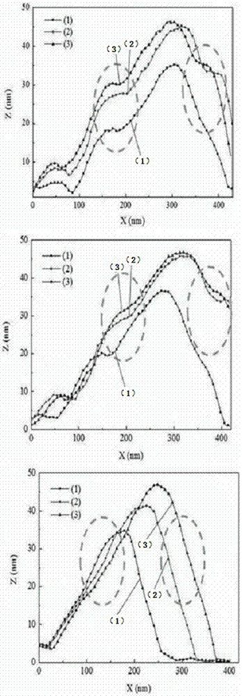
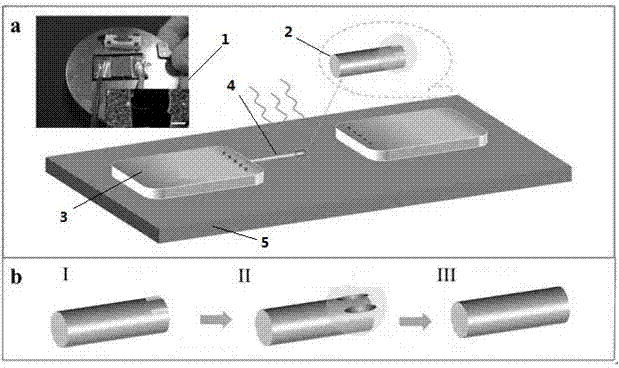
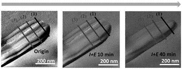
[0036] 6. Using a probe with a d...
Embodiment 2
[0039] 1. Cut the clean glass sheet into 2×3 cm samples, then soak it in fatty alcohol polyoxyethylene ether sodium sulfate solution, and ultrasonicate it in a water bath at 35°C for 10 minutes; then rinse it with deionized water for 3 times and soak it in deionized Sonicate in water for 15 min.
[0040] 2. Take out the sample, soak it in acetone solution at room temperature for 10 minutes, take it out and rinse it with deionized water three times, dry it with nitrogen, and put it in a desiccator for later use.
[0041] 3. Place the above prepared sample in an ozone generating device for 15 minutes.
[0042] 4. Use a high-resolution magnetron ion sputtering device to coat a silver film on the surface of the glass under the conditions of a sputtering current of 15mA and a sputtering time of 200s.
[0043] 5. Under the protection of nitrogen atmosphere, the sample was annealed at 300°C for 1 hour, and a bright silver film could be observed on the glass surface after annealing. ...
PUM
| Property | Measurement | Unit |
|---|---|---|
| diameter | aaaaa | aaaaa |
| diameter | aaaaa | aaaaa |
| diameter | aaaaa | aaaaa |
Abstract
Description
Claims
Application Information