Dual-concave high-voltage ceramic capacitor and manufacturing process thereof

A high-voltage ceramic and capacitor technology, applied in the field of high-voltage ceramic capacitors and manufacturing processes, can solve the problems of unadjustable electrode size, uneven electrode thickness, unadjustable capacitance, etc., to reduce the risk of tip discharge, high charge density, and reduced The effect of the risk of small tip discharge

Inactive Publication Date: 2017-06-30
KUSN WANFENG ELECTRONICS
View PDF5 Cites 4 Cited by
  • Summary
  • Abstract
  • Description
  • Claims
  • Application Information

AI Technical Summary

Problems solved by technology

Because traditional ceramic capacitors use the process of printing conductive paste and then sintering to prepare electrodes, when the patent CN202268250U dielectric structure prints conductive paste, due to the difference in the depth of the ceramic substrate, the force of the scraper is different, and the conductive paste will deposit in the concave shape, resulting in electrode thickness. Uneven, waste of conductive paste
Patent CN104167290A proposes a concave high-voltage ceramic capacitor, the dielectric structure of which is also concave, and a cylindrical vacancy is formed symmetrically on the upper and lower circular planes of the cylindrical dielectric, and its electric polarization process adopts the overall chemical deposition process. After the copper layer is deposited on the entire ceramic substrate, the copper layer on the outer surface of the ceramic substrate cylinder is ground to form an electrode. The thickness of the electrode layer is uniform. The disadvantage is that the electrode completely covers the circular surface of the substrate, and the electrode size cannot be adjusted, that is, the capacitance. It cannot be adjusted. In addition, the process of edging is easy to cause chipped corners of the substrate due to mechanical external force, which artificially causes process defects.

Method used


Image

  • Dual-concave high-voltage ceramic capacitor and manufacturing process thereof
  • Dual-concave high-voltage ceramic capacitor and manufacturing process thereof
  • Dual-concave high-voltage ceramic capacitor and manufacturing process thereof

Examples


Embodiment 1

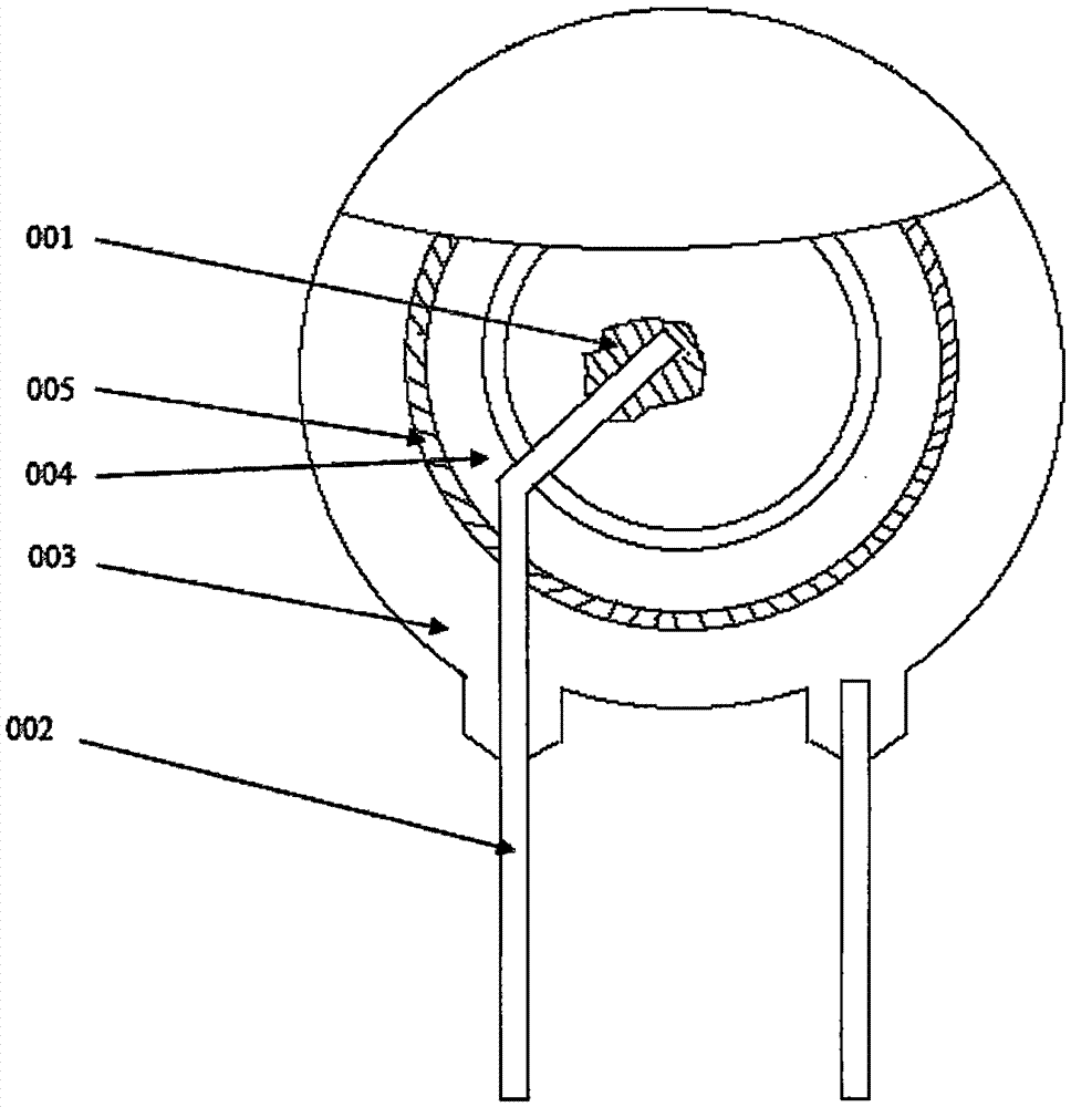
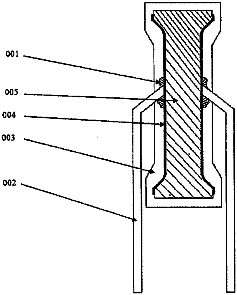
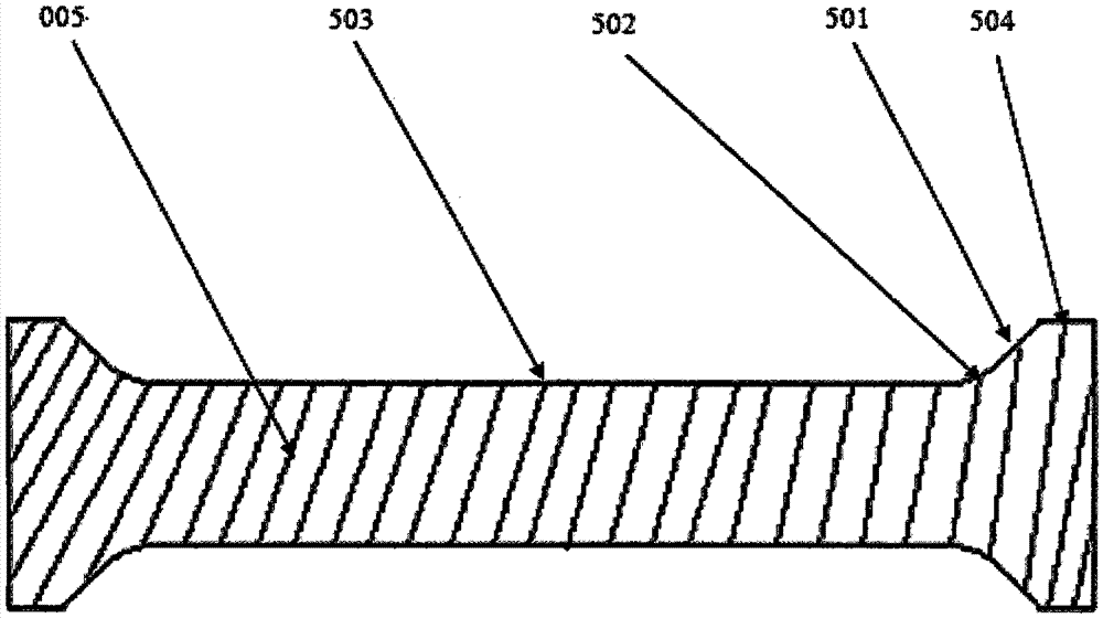
[0028] Embodiment 1, see attached figure 1 , 2, 3, and 4, a double-concave high-voltage ceramic capacitor related to the present invention includes solder 001, lead 002, resin encapsulation layer 003, electrode layer 004 and ceramic dielectric substrate 005, and the ceramic dielectric The substrate 005 is a centrally symmetrical cylinder with a frustum-shaped vacancy on the upper and lower bottom surfaces. The axis of the vacant frustum coincides with the axis of the ceramic dielectric substrate 005. The area of ​​the circular surface of the circular frustum is smaller than the area of ​​the bottom surface of the cylinder. The slope 501 on the side of the vacant circular frustum is smaller There is a transitional surface 502 with an arc section at the junction of the area circular surfaces, that is, the thickness of the central part of the ceramic dielectric substrate 005 is thinner than the edge, and there is a shape between the circular surface 503 at the center of the botto...


PUM


Abstract

The invention relates to a dual-concave high-voltage ceramic capacitor and a manufacturing process thereof. A ceramic dielectric substrate of the capacitor is shaped like a cylinder, two truncated cone-shaped gaps are formed in the cylinder, and then two concave portions are formed, that is to say, the thickness of the edge of the ceramic substrate is greater than that of the center. A transition surface with an arc line being the cross section is arranged between a round surface in the center of the ceramic substrate and a concave inclined surface of a truncated cone-shaped side surface. The ceramic substrate is provided with an electrode. The electrode is divided into three layers, wherein the top layer is tin alloy. The electrode is welded to a lead wire. Epoxy resin wraps the substrate, the electrode and part of the lead wire. The manufacturing process of the capacitor includes ceramic substrate manufacturing, electric polarization, lead wire welding, coating, printing, and testing. The electrode of the capacitor is manufactured through magnetron sputtering, and can be freely controlled in size. Through the design of the transition surface in the substrate concave parts, point discharge risks of the electrode are reduced, the over-voltage resistance of the capacitor is further improved, and the capacitor can become miniature. Through the design of a copper-tin alloy layer, the electrode can still be welded if part of the electrode is oxidized.

Description

technical field [0001] The invention relates to the field of ceramic capacitors, in particular to a high-voltage ceramic capacitor with a double-concave dielectric and adjustable electrode size and a manufacturing process. Background technique [0002] As a basic passive component, ceramic capacitors are widely used in power supplies, home appliances, automobiles and other equipment for filtering, oscillation and coupling. Traditional ceramic capacitors are discrete components, mainly cylindrical in shape. The molding process is simple, and the density of the green sheet after molding is uniform. It is convenient for sintering, printing electrodes, welding leads, and large-scale production. The current miniaturization development trend of electronic components is obvious. Patent CN202268250U discloses a high-voltage ceramic capacitor dielectric structure. The dielectric is double-concave. The breakdown mode of plate-type high-voltage ceramic capacitors is generally electrod...

Claims


Application Information

Patent Timeline
IPC IPC(8): H01G4/008H01G4/30H01G4/12H01G4/224H01G13/00
CPCH01G4/008H01G4/12H01G4/224H01G4/30H01G13/003
Inventor 李伟力李国正徐晓阙华昌方弋卜顺梁
Owner KUSN WANFENG ELECTRONICS
Why Eureka
Try Eureka