Electroforming method of slotted waveguide
A technology of electroforming and waveguide, applied in the direction of electroforming, electrolysis, etc., to achieve the effect of simplifying the process, avoiding many burrs, and no processing stress
- Summary
- Abstract
- Description
- Claims
- Application Information
AI Technical Summary
Problems solved by technology
Method used
Image
Examples
Embodiment Construction
[0024] The slotted waveguide to be prepared is as Figure 10 As shown, the following preparation process is adopted:
[0025] Step 1: Prepare the core mold. The core mold consists of two parts, the lower structure 4 and the upper structure 7. The lower structure 4 of the core mold is a rectangular nickel layer structure with a thickness of L2. The adjacent rectangular nickel layer structures have the same length. The upper layer of the core mold Structure 7 is a micro-cuboid column array structure with a thickness of L4, and the specific preparation method is as follows:
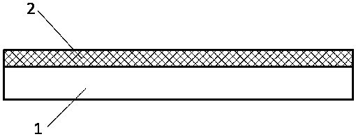
[0026] Step 1.1: coating a first layer of photoresist 2 with a thickness of L1 on the substrate 1;
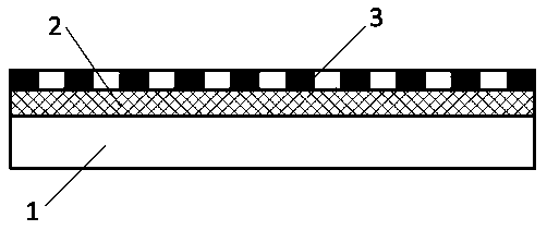
[0027] Step 1.2: Place the substrate 1 after the first coating in step 1.1 on the stage of the photolithography machine, and use the first mask plate 3 to perform the first exposure;
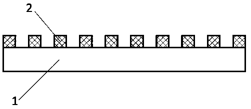
[0028] Step 1.3: Put the substrate 1 after the first exposure in step 1.2 into the developing solution for the first develo...
PUM
| Property | Measurement | Unit |
|---|---|---|
| surface roughness | aaaaa | aaaaa |
Abstract
Description
Claims
Application Information


