Scalable optical network-on-chip architecture and communication method based on double-layer layout

A network structure and layout technology, applied in the field of communication, can solve the problems of insufficient waveguide layout in the optical switching unit, increase in the average number of communication hops, and large network cross loss, etc., to achieve high bandwidth, high energy utilization, and low network loss Effect

Active Publication Date: 2019-05-21
XIDIAN UNIV
View PDF7 Cites 0 Cited by
  • Summary
  • Abstract
  • Description
  • Claims
  • Application Information

AI Technical Summary

Problems solved by technology

However, the shortcomings of this system are: the layout of the waveguide in the optical switching unit is not optimized enough, resulting in a large crossover loss of the optical on-chip network, limited expansion capability, and low application value
However, the disadvantages of this method are: with the expansion of the integration scale based on the Mesh structure, the diameter of the network increases, the average number of communication hops increases, and the time delay overhead of using this communication method to transmit from near to far is relatively large
However, the shortcomings of this method are: the blocking problem is solved through the retransmission mechanism, the network flexibility is low, and the method ignores the network communication for specific applications

Method used


Image

  • Scalable optical network-on-chip architecture and communication method based on double-layer layout
  • Scalable optical network-on-chip architecture and communication method based on double-layer layout
  • Scalable optical network-on-chip architecture and communication method based on double-layer layout

Examples


Embodiment Construction

[0039] The present invention will be described in further detail below in conjunction with the accompanying drawings.

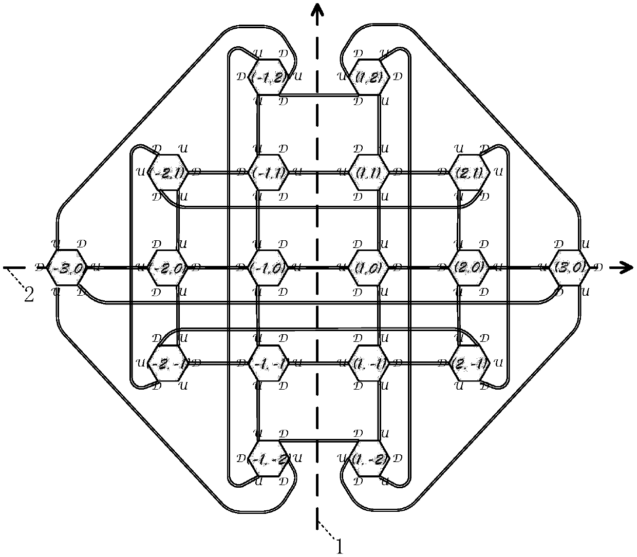
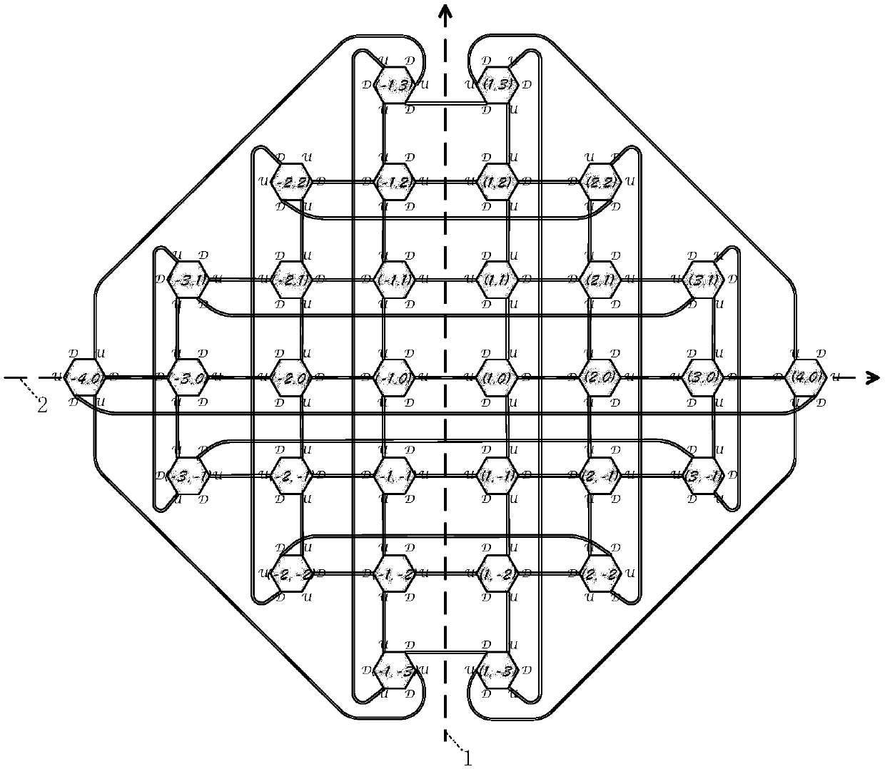
[0040] The device of the present invention includes upper and lower silicon substrates and 2N etched on the upper and lower silicon substrates. 2 A six-port optical router, 4N 2 Root optical waveguide, 4N connected by six-port optical router and optical waveguide 2 Intellectual property IP cores, where N is a positive integer greater than or equal to 3.

[0041] 2N2 A six-port optical router is composed of two kinds of mirror-symmetrical staggered six-port optical routers arranged alternately. Two local ports in each six-port optical router are respectively connected to two intellectual property IP cores, and the remaining four are interconnected. The connection port is connected with other six-port optical routers through waveguides to realize the reception and forwarding of optical signals in the network.

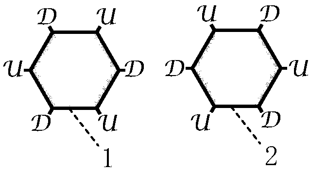
[0042] Two kinds of staggered-layer six-port op...


PUM


Abstract

The invention discloses an expandable optical network-on-chip structure based on double-layer layout and a communication method thereof and mainly solves the problem that in an existing optical network-on-chip structure is high in cross loss and relatively high in communication time delay cost. The structure comprises optical routers, optical waveguides and intellectual property IP cores. Each six-port optical router is connected with two intellectual property IP cores and four optical waveguides. The optical waveguides are etched on upper layer silicon substrates and lower layer silicon substrates according to the positions of the connected router ports. The communication method comprises the steps of establishing a coordinate system in an expandable optical network-on-chip; determining transmission paths of signals; configuring optical router ports on the transmission paths; sending optical signals; and receiving and processing the optical signals. According to the structure and the method, the layout of the optical network-on-chip structure is effectively optimized, and the expandability and communication efficiency of the optical network-on-chip are improved.

Description

technical field [0001] The present invention belongs to the technical field of communication, and further relates to a scalable optical network-on-chip network structure and a communication method based on a double-layer layout in the technical field of multi-core node interconnection in Optical Network-on-Chip (ONoC). The present invention is based on an expandable optical on-chip network structure and a communication method based on a double-layer layout, and is used to build an on-chip intellectual property (Intellectual Property, IP) core interconnection network, realize information transmission between IP cores, and improve on-chip network communication efficiency. Background technique [0002] Compared with traditional on-chip electrical interconnection methods, optical interconnection through optical signals has the advantages of higher bandwidth density, smaller communication delay, lower system power consumption, and smaller network crosstalk. In recent years, the c...

Claims


Application Information

Patent Timeline
Patent Type & Authority Patents(China)
IPC IPC(8): H04L12/931H04L12/933H04Q11/00
CPCH04L49/109H04L49/357H04Q11/0005
Inventor 顾华玺黄蕾杨银堂朱樟明齐世雄王琨
Owner XIDIAN UNIV
Why Eureka
Try Eureka