A method for rapid preparation of large-area surface-enhanced Raman scattering substrates

A surface-enhanced Raman and large-area technology, applied in Raman scattering, material excitation analysis, instruments, etc., can solve the problems of poor SERS signal consistency, high cost, and low preparation efficiency, and achieve enhanced effect consistency, size and The effect of uniform distribution and pure background signal

Inactive Publication Date: 2019-07-12
XIAMEN UNIV
View PDF3 Cites 0 Cited by
  • Summary
  • Abstract
  • Description
  • Claims
  • Application Information

AI Technical Summary

Problems solved by technology

The surface morphology of rough metal electrodes prepared by electrochemical roughening is disordered, and the size and shape are not easy to control, resulting in poor consistency of SERS signals and cannot be used for quantitative measurement
The nanoparticle synthesis method has the disadvantages that the nanoparticles are easy to agglomerate and unstable, and the residual chemical impurities in the synthesis process will cause a large background spectrum of the SERS substrate, which cannot be used for the detection of trace substances
Micro-nano etching methods mainly include photolithography, electron beam etching, and focused ion beam etching. Although micro-nano etching can produce uniform micro-nano structure arrays, such methods have low preparation efficiency and low cost. High, cumbersome preparation process

Method used


Image

  • A method for rapid preparation of large-area surface-enhanced Raman scattering substrates
  • A method for rapid preparation of large-area surface-enhanced Raman scattering substrates
  • A method for rapid preparation of large-area surface-enhanced Raman scattering substrates

Examples


Embodiment Construction

[0029] Below by embodiment the content of the present invention is specified:

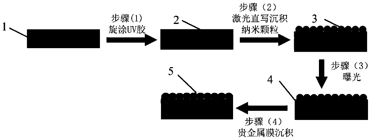
[0030] Please check figure 1 , a method for rapidly preparing a large-area surface-enhanced Raman scattering substrate, comprising:

[0031] 1) Spin-coat UV glue on a transparent substrate: In this embodiment, a transparent quartz slide is used as the transparent substrate 1; first, the quartz slide is placed in an ultrasonic cleaner, and acetone, isopropanol, Ultrasonic cleaning of the transparent substrate 1 with water for 1 min, and the transparent substrate 1 is cleaned; then, the cleaned transparent substrate 1 is placed on a homogenizer and spin-coated with UV glue. . The purpose of spin-coating UV glue on the transparent substrate 1 is to better fix the subsequently deposited nanoparticles on the transparent substrate 1 .

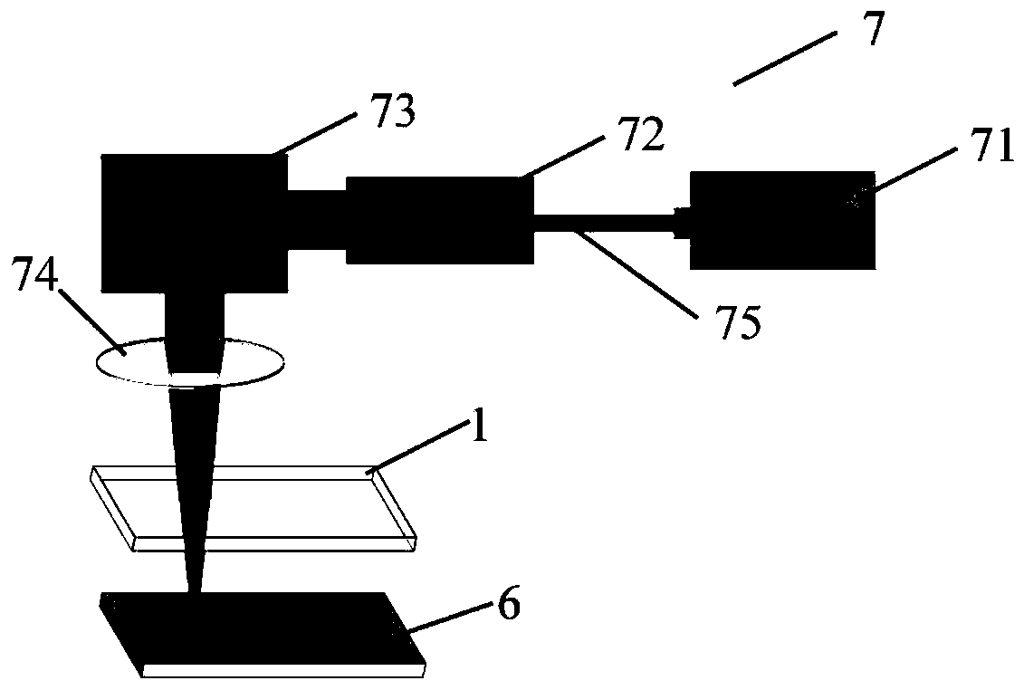
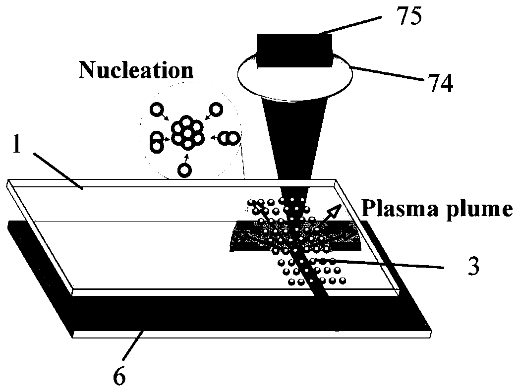
[0032] 2) Depositing the nanoparticles 3 of the target material 6 on the transparent substrate 1 by laser direct writing. figure 2 A schematic diagram of a device fo...


PUM

PropertyMeasurementUnit
thicknessaaaaaaaaaa
wavelengthaaaaaaaaaa
frequencyaaaaaaaaaa

Abstract

The invention discloses a method for rapidly preparing large-area surface-enhanced Raman scattering substrate. The method comprises the steps that 1, light solidification glue is prepared on a transparent substrate; 2, the transparent substrate with the light solidification glue is arranged on the upper portion of a target material, a laser pulse penetrates through the transparent substrate and the light solidification glue and then is focused on the target material surface, and the target material absorbs the laser pulse and then generates nano-particles which is deposited on the light solidification glue surface; 3, the light solidification glue is cured through exposure, and then the deposited nano-particles are fixed to the transparent substrate; 4, a metal thin film is deposited on the nano-particles to form a metal nanostructure, and the surface-enhanced Raman scattering substrate is obtained. Accordingly, pulse laser is used for directly depositing the nano-particles generated by the target material onto the transparent substrate surface, the sizes of the nano-particles can be selected by regulating the distance between the target material and the transparent substrate, the controllability is good, the large-area SERS substrate can be prepared in a low-cost, efficient and rapid mode, and the prepared SERS substrate is high in sensitivity, good in consistency and pure in background signal.

Description

technical field [0001] The invention belongs to the technical field of Raman detection, and in particular relates to a method for rapidly preparing a large-area surface-enhanced Raman scattering substrate. Background technique [0002] Raman spectroscopy is a scattering spectrum that contains material structure information. It is the light scattering caused by the inelastic collision between incident photons and molecular vibration and rotation quantized energy level resonance. It is an effective means of material identification. However, due to the weak Raman scattering intensity, (usually 10 of the incident light -6 ), and the Raman scattering cross-section is much smaller than the fluorescence scattering cross-section, resulting in the weak Raman scattering signal is often lost in the fluorescence signal, which limits the application of Raman spectroscopy. Surface-enhanced Raman scattering (SERS) is an effective means to enhance Raman signals, and effectively solves the ...

Claims


Application Information

Patent Timeline
Patent Type & Authority Patents(China)
IPC IPC(8): G01N21/65
CPCG01N21/658
Inventor 张陈涛张建寰林坤李姗文黄元庆
Owner XIAMEN UNIV
Why Eureka
Try Eureka