Grooved gate enhanced GaN transistor device based on nano channel

An enhanced transistor technology, applied in semiconductor devices, electrical components, circuits, etc., can solve the problems of large on-resistance of devices, short gate length, etc.

Active Publication Date: 2017-07-25
THE 13TH RES INST OF CHINA ELECTRONICS TECH GRP CORP
View PDF4 Cites 6 Cited by
  • Summary
  • Abstract
  • Description
  • Claims
  • Application Information

AI Technical Summary

Problems solved by technology

However, with the continuous shrinking of the device size and the shorter gate length, the short channel effect of the traditional planar high electron mobility transistor becomes more and more obvious.
In 2013, Ki-Sik Im and others prepared an enhanced AlGaN / GaN MISFET with a single nanochannel, with a threshold voltage of 2.1V. The device structure uses a common gate structure. In order to realize an enhanced device, the nanochannel width is only 50nm , and both ends of the nanochannel extend to the source and drain electrode regions, so the device has a large on-resistance

Method used


Image

  • Grooved gate enhanced GaN transistor device based on nano channel
  • Grooved gate enhanced GaN transistor device based on nano channel
  • Grooved gate enhanced GaN transistor device based on nano channel

Examples


Embodiment 1

[0028] Embodiment 1: A groove-gate enhanced GaN transistor device based on a single nanochannel.

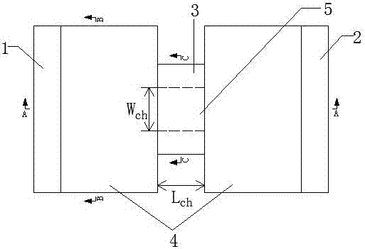
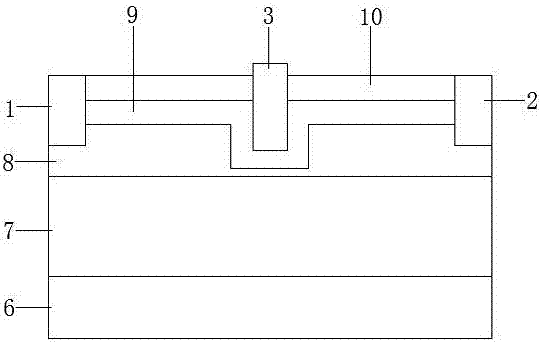
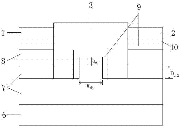
[0029] figure 1 It is a top view of an overall structure of an embodiment of the present invention, figure 2 , image 3 with Figure 4 respectively figure 1 Sectional views of plane A-A, plane B-B and plane C-C. The groove gate enhanced GaN transistor device based on the single nanochannel 5 in this embodiment includes a substrate layer 6, a GaN buffer layer 7, an AlGaN barrier layer 8, a gate dielectric layer 9, a passivation layer 10 and a source electrode from bottom to top 1. Drain electrode 2 and gate electrode 3.

[0030] The material used for the substrate layer 6 is sapphire, SiC or GaN.

[0031] Above the substrate layer 6 is a GaN buffer layer 7 with a thickness of 0.5-2.5 μm.

[0032] Above the buffer layer is an AlGaN barrier layer 8 with a thickness of 10-20 nm and an Al composition of 15%-30%.

[0033] The AlGaN barrier layer 8 and the GaN buffer layer 7 fo...

Embodiment 2

[0039] Embodiment 2: a groove-gate enhanced GaN transistor device based on a single nanochannel.

[0040] Such as Figure 5 As shown, the groove gate enhanced GaN transistor device based on the single nanochannel 5 of this embodiment has the same structure as that of the first embodiment, but the length L of the nanochannel 5 ch for L ch >Gate length L g .

Embodiment 3

[0041] Embodiment 3: Recessed gate enhanced GaN transistor device based on multi-nanometer channels.

[0042] Such as Image 6 As shown, the groove gate enhanced GaN transistor device based on multiple nanochannels in this embodiment has the same structure as that in Embodiment 1, but the number n of the nanochannels 5 is n>1.


PUM


Abstract

The invention discloses a grooved gate enhanced GaN transistor device based on a nano channel and relates to the technical field of microelectronic devices. The grooved gate enhanced GaN transistor device comprises, from bottom to top, a substrate layer, a GaN buffer layer, an AlGaN barrier layer, a gate dielectric layer, a passivation layer, a source, a drain and a gate. The heterojunction under the gate of an AlGaN/GaN high-electron-mobility transistor device is etched to form the nano channel such that no two-dimensional electron gas exists in the regions on both sides of the nano channel. The gate wraps the top and two sidewalls of the nano channel. The gate modulates the electrons in the nano channel from three directions so as to have good control ability and well suppress a short channel effect. When the nano channel has a small width, the two-dimensional electron gas in the channel is exhausted and the device is enhanced. The combined effect of the nano channel and grooved gate can ensure that the device has a large nano-channel width while enhanced, and reduces the on-resistance.

Description

technical field [0001] The invention relates to the technical field of microelectronic devices, in particular to a groove gate enhanced GaN transistor device based on nano-channels. Background technique [0002] The wide bandgap semiconductor material GaN has the advantages of high critical breakdown electric field, high electron saturation velocity, good thermal stability and strong radiation resistance, especially AlGaN / GaN heterostructure materials due to spontaneous polarization and piezoelectric Due to its extremely high two-dimensional electron gas concentration and electron mobility, it is considered to be an excellent material for the preparation of high-temperature, radiation-resistant, high-frequency, high-power microwave power devices, high-speed, high-voltage power switching devices, and radiation-resistant high-speed digital circuits. [0003] Due to the existence of polarization effects, AlGaN / GaN high electron mobility transistors are usually depletion-mode de...

Claims


Application Information

Patent Timeline
Patent Type & Authority Applications(China)
IPC IPC(8): H01L29/778H01L29/20H01L29/423H01L29/06
CPCH01L29/0603H01L29/0684H01L29/2003H01L29/4236H01L29/7786H01L29/7788Y02B70/10
Inventor 周幸叶冯志红吕元杰谭鑫王元刚宋旭波徐鹏
Owner THE 13TH RES INST OF CHINA ELECTRONICS TECH GRP CORP
Why Eureka
Try Eureka