Ionic type memristor having quantum conductance effect

An ion-type, memristor technology, applied in semiconductor devices, circuits, electrical components, etc., can solve problems such as unfavorable applications of strong artificial intelligence devices

Inactive Publication Date: 2017-07-28
BEIHANG UNIV
View PDF3 Cites 28 Cited by
  • Summary
  • Abstract
  • Description
  • Claims
  • Application Information

AI Technical Summary

Problems solved by technology

Although quantum conductance and other effects have been realized in the above research process, its conductance behavior is very different from the information exchange mechanism of the human brain, which is not conducive to the application in strong artificial intelligence devices such as brain-like computing devices and neuromorphic networks.

Method used


Image

  • Ionic type memristor having quantum conductance effect
  • Ionic type memristor having quantum conductance effect
  • Ionic type memristor having quantum conductance effect

Examples


Embodiment 1

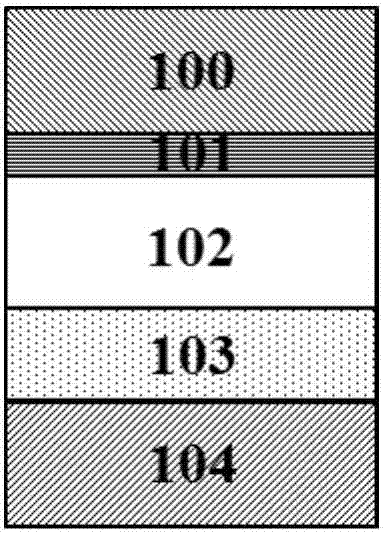
[0042] In this embodiment, it is based on the structure of "top electrode / tunneling layer / oxide layer / ion-doped layer / bottom electrode". As shown in FIG. 2( a ), the structure consists of five layers from bottom to top: bottom electrode 104 , ion-doped layer 103 , oxide layer 102 , tunneling layer 101 and top electrode 100 . The bottom electrode 104 is made of platinum with a thickness of 100 nanometers; the ion-doped layer 103 is made of lithium-ion-doped hafnium dioxide with a thickness of 30 nanometers; the oxide layer 102 is made of 30 nanometers of hafnium dioxide; the thickness of the tunneling layer 101 is selected to be 0.34 nanometer single-layer graphene; the top electrode 100 selects 100 nanometer titanium nitride.

[0043] The structure is prepared layer by layer on the substrate from bottom to top by using methods such as pulsed laser deposition, atomic layer deposition, magnetron sputtering, electron beam evaporation, etch transfer. First, a layer of metal plati...

Embodiment 2

[0046] In this embodiment, it is based on the structure of "top electrode / ion-doped layer / oxide layer / tunneling layer / bottom electrode". As shown in FIG. 2( b ), the structure consists of five layers from bottom to top: bottom electrode 104 , tunneling layer 101 , oxide layer 102 , ion-doped layer 103 and top electrode 100 . The bottom electrode 104 is copper with a thickness of 100 nanometers; the tunneling layer 101 is a single-layer graphene with a thickness of 0.34 nanometers; the oxide layer 102 is tantalum pentoxide with a thickness of 30 nanometers; the ion-doped layer 103 is doped with Na ions Tantalum pentoxide with a thickness of 30 nanometers; the top electrode 100 is tantalum nitride with a thickness of 100 nanometers.

[0047] The structure is prepared layer by layer on the substrate from bottom to top by laser pulse deposition, atomic layer deposition, magnetron sputtering, chemical vapor deposition, electron beam evaporation and other methods. First, a layer of...

Embodiment 3

[0050] In this embodiment, it is based on the structure of "top electrode / oxide layer / tunneling layer / ion-doped layer / bottom electrode". As shown in FIG. 2( c ), the structure consists of five layers from bottom to top: bottom electrode 104 , ion-doped layer 103 , tunneling layer 101 , oxide layer 102 and top electrode 100 . The bottom electrode 104 is gold with a thickness of 100 nanometers; the ion-doped layer 103 is lithium cobalt oxide with a thickness of 30 nanometers; the tunneling layer 101 is a single-layer molybdenum disulfide with a thickness of 0.4 nanometers; silicon dioxide; the top electrode 100 selects 100 nanometers of platinum.

[0051] The structure is prepared layer by layer on the substrate from bottom to top by using methods such as pulsed laser deposition, atomic layer deposition, magnetron sputtering, transfer technology, and electron beam evaporation. First, a layer of metal gold is prepared on a flat and clean substrate by electron beam evaporation as...


PUM


Abstract

The invention discloses an ionic type memristor having a quantum conductance effect. The ionic type memristor has a "sandwich" structure or a field effect transistor structure. The ionic type memristor having the "sandwich" structure is composed of a top electrode, a tunneling layer, an oxide layer, an ion-doped layer and a bottom electrode. The specific structure is as follows: "the top electrode/the tunneling layer/the oxide layer/the ion-doped layer/the bottom electrode", "the top electrode/the oxide layer/the ion-doped layer/the tunneling layer/the bottom electrode" and "the top electrode/the oxide layer/the tunneling layer/the ion-doped layer/the bottom electrode". The top electrode has a thickness of 30-100 nm. The tunneling layer has a thickness of 0.34-5 nm. The oxide layer has a thickness of 10-40 nm. The ion-doped layer has a thickness of 10-40 nm. The bottom electrode has a thickness of 30-100 nm. The ionic type memristor of the invention can produce a memristive effect based on alkali metal or alkali metal ionic migration; and can achieve a quantum conductance effect using a tunneling effect when ions penetrate through the tunneling layer or a quantum size effect of a nanowire channel on the ions, so that multiple quantum states are observed.

Description

technical field [0001] The invention provides an ion-type memristor with low energy consumption, multi-resistance states and quantum conductance effect, which belongs to the technical field of brain-like computing devices. Background technique [0002] In recent years, artificial intelligence has become a hot spot of research and competition around the world. Artificial intelligence is mainly divided into weak artificial intelligence and strong artificial intelligence. Weak artificial intelligence has been gradually realized. How to realize strong artificial intelligence is the focus and difficulty of current research, and brain-like computing is considered to be one of the important ways to realize strong artificial intelligence. Brain-inspired computing refers to devices, models and methods that simulate, simulate and learn from the structure of the brain's nervous system and information processing processes, and its goal is to manufacture brain-inspired smart chips. Bra...

Claims


Application Information

Patent Timeline
Patent Type & Authority Applications(China)
IPC IPC(8): H01L45/00H01L29/66H01L29/775
CPCH01L29/66977H01L29/775H10N70/245
Inventor 黄安平胡琪
Owner BEIHANG UNIV
Why Eureka
Try Eureka