Preparation method for preparing interface composed of ordered microstructure and controllable chemistry and application thereof
A technology of microstructure and chemical composition, applied in the manufacture of microstructure devices, microstructure devices, microstructure technology, etc.
- Summary
- Abstract
- Description
- Claims
- Application Information
AI Technical Summary
Problems solved by technology
Method used
Image
Examples
preparation example Construction
[0034] The method for preparing ordered microstructure and chemical composition substrate interface provided by the present invention specifically includes:
[0035] The first step, silicon wafer cleaning;
[0036] The second step is the preparation of the surface structure;
[0037] The third step is the construction of the hydrophobic surface.
[0038] The first step is further specified as etching a smooth silicon wafer (P-type, crystal orientation 100) or silicon with a micron structure (using a mask to etch P-type, crystal orientation 100 smooth) Silicon obtained) were respectively immersed in acetone and ethanol for 15 minutes, rinsed with water, then immersed in a solution of 98% sulfuric acid and hydrogen peroxide with a volume ratio of 3:1, heated at 80°C for 30 minutes, taken out and rinsed with a large amount of water. At this time, the silicon wafer is hydrophilic.
[0039] When using a smooth silicon wafer, the first step is to prepare the surface structure of ...
Embodiment 1
[0049] Embodiment 1 Nanowire array surface structure
[0050] Soak the silicon wafer (type P, crystal orientation 100) in washing solution, acetone, and ethanol for 15 minutes, rinse with water respectively, then immerse in a solution with a volume ratio of sulfuric acid and hydrogen peroxide of 3:1, and heat at 80°C for 10 minutes. Remove and rinse with plenty of water.
[0051] Weigh 0.1699g of silver nitrate and put it into a plastic beaker, absorb 10ml of hydrofluoric acid with a syringe, add water to make a 50ml mixed reaction solution, pour it into a polytetrafluoro reactor, add cleaned silicon wafers, cover and place at 50 Heat the reaction in an oven at ℃ for 20 minutes. Because the wall of the PTFE reactor is relatively thick, in order to ensure the reaction effect, the reaction solution should be preheated in an oven at 50 ℃ for 10 minutes in advance. After the reaction, the silicon wafer was taken out, soaked in nitric acid for about 15s to remove the gray silver f...
Embodiment 2
[0052] Example 2 Micro-nano composite array surface structure
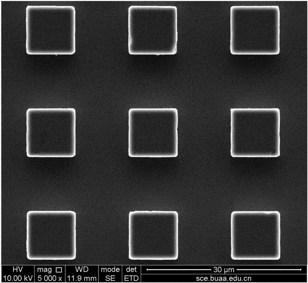
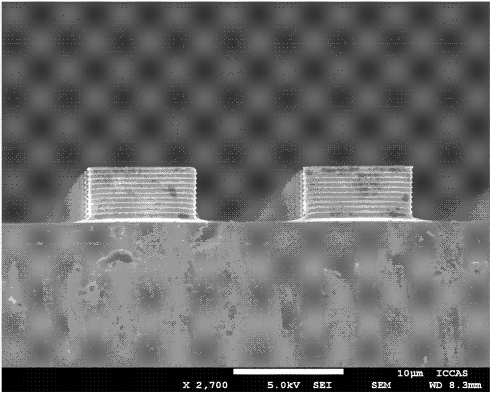
[0053] Silicon with a micron structure (obtained by etching P-type, crystal orientation 100 smooth silicon using a mask plate in Peking University Micro-Nano Processing Laboratory) (such as figure 2 and image 3 Shown) immerse in washing liquid, acetone, and ethanol and sonicate for 15 minutes, rinse with water respectively, then immerse in a solution with a volume ratio of sulfuric acid and hydrogen peroxide of 3:1, heat at 80°C for 10 minutes, take it out and rinse with a large amount of water.
[0054] Weigh 0.1699g of silver nitrate and put it into a plastic beaker, absorb 10ml of hydrofluoric acid with a syringe, add water to make a 50ml mixed reaction solution, pour it into a polytetrafluoroethylene reactor, and add a cleaned silicon chip with a micro-column structure , column width / column height / column spacing = 10 / 5 / 10μm, cover and place in a 50°C oven to heat and react for 10min, here control the corros...
PUM
| Property | Measurement | Unit |
|---|---|---|
| diameter | aaaaa | aaaaa |
Abstract
Description
Claims
Application Information
 - R&D
- Intellectual Property
- Life Sciences
- Materials
- Tech Scout
- Unparalleled Data Quality
- Higher Quality Content
- 60% Fewer Hallucinations
Browse by: Latest US Patents, China's latest patents, Technical Efficacy Thesaurus, Application Domain, Technology Topic, Popular Technical Reports.
© 2025 PatSnap. All rights reserved.Legal|Privacy policy|Modern Slavery Act Transparency Statement|Sitemap|About US| Contact US: help@patsnap.com


