Porous-DBR-based InGaN-based resonant cavity enhanced detector chip

A detector chip and resonant cavity technology, applied in semiconductor devices, electrical components, circuits, etc., can solve the problems of increasing the drift time of photogenerated carriers, restricting the response speed of the detector, and the effective thickness of the InGaN layer. Simple and controllable, improved epitaxial quality, low cost effect

Inactive Publication Date: 2017-08-15
INST OF SEMICONDUCTORS - CHINESE ACAD OF SCI
View PDF4 Cites 14 Cited by
  • Summary
  • Abstract
  • Description
  • Claims
  • Application Information

AI Technical Summary

Problems solved by technology

However, the effective thickness of the InGaN layer obtained by this method is still limited.
In addition, increasing the quantum efficiency of the detector by increasi

Method used


Image

  • Porous-DBR-based InGaN-based resonant cavity enhanced detector chip
  • Porous-DBR-based InGaN-based resonant cavity enhanced detector chip
  • Porous-DBR-based InGaN-based resonant cavity enhanced detector chip

Examples


Embodiment Construction

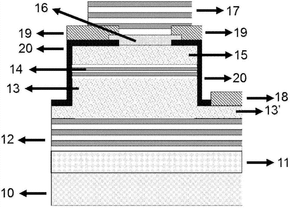
[0023] see figure 1 As shown, the present invention provides a porous DBR-based InGaN-based resonator-enhanced detector chip. This InGaN-based resonant cavity detector structure consists of:

[0024] A substrate 10, a planar sapphire substrate or a patterned sapphire substrate. Other substrates that can be used for epitaxy include silicon, silicon carbide or glass;

[0025] A buffer layer 11 is formed on the upper surface of the substrate 10 . This layer uses high-purity ammonia gas as a nitrogen source, and trimethylgallium or triethylgallium as a Ga source. First, a GaN nucleation layer is grown at a low temperature, and then an unintentionally doped GaN layer is grown at a high temperature. Others that can be used as a buffer layer are graphene or zinc oxide;

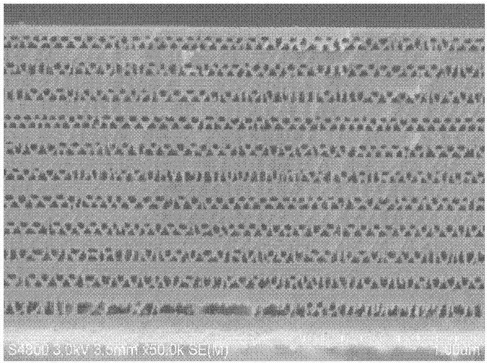
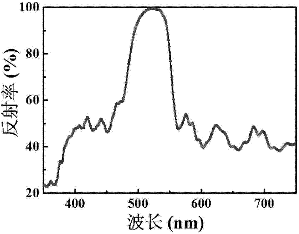
[0026] A bottom porous DBR layer 12 is formed on the upper surface of the buffer layer 11 . This layer is obtained by electrochemical etching of alternately lightly and heavily doped GaN layers, the dopant is si...


PUM


Abstract

The invention relates to a porous-DBR-based InGaN-based resonant cavity enhanced detector chip comprising a substrate, a buffer layer formed on the substrate, a bottom porous DBR layer formed on the buffer layer, an n type GaN layer formed on the bottom porous DBR layer, an active region formed on the n type GaN layer, a p type GaN layer formed in the active region, a side wall passivation layer, a transparent conductive layer, an n electrode, a p electrode, and a top dielectric DBR layer. The one side of the n type GaN layer is formed downwardly to form a table board and a protrusion is formed at the other side of the n type GaN layer. The side wall passivation layer is formed at the upper surface of the p type GaN layer and the side walls of the protruding n type GaN layer, the active region, and the p type GaN layer; and a window is formed in the middle of the side wall passivation layer formed at the upper surface of the p type GaN layer. The transparent conductive layer is formed at the upper surfaces of the side wall passivation layer and the p type GaN layer at the window. The n electrode is formed on the table board of the n type GaN layer. The p electrode is manufactured around the upper surface of the side wall passivation layer. And the top dielectric DBR layer is formed on the transparent conductive layer and the p electrode.

Description

technical field [0001] The invention relates to a vertical cavity surface resonator enhanced photodetector, in particular to an InGaN-based vertical cavity surface resonant enhanced detector chip based on a porous Bragg reflector (DBR). Background technique [0002] At present, visible light communication has shown broad application prospects in the fields of smart homes and smart cities. As an important part of the visible light communication system, the photoelectric conversion efficiency and response speed of the light receiving end will directly restrict the transmission distance and transmission rate of visible light communication. At present, the optical receiving end mostly adopts traditional Si-based or GaAs, GaP-based and other commercial semiconductor visible light detectors, but such traditional detectors are susceptible to background signal interference in outdoor complex communication environments. GaN and its ternary compounds AlGaN and InGaN have the characte...

Claims


Application Information

Patent Timeline
IPC IPC(8): H01L31/0232H01L31/0304H01L31/112
CPCH01L31/02327H01L31/03042H01L31/03044H01L31/112H01L31/03048H01L31/035236H01L31/036H01L31/109H01L31/02161
Inventor 刘磊杨超赵丽霞
Owner INST OF SEMICONDUCTORS - CHINESE ACAD OF SCI
Why Eureka
Try Eureka