Self-driven near infrared photodetector based on potassium sulfate quasi-one-dimensional nanostructure and preparation method thereof

A nanostructure, near-infrared light technology, applied in the direction of circuits, electrical components, semiconductor devices, etc., can solve problems such as limited promotion, high equipment conditions, and production costs, and achieve easy integration, reduced preparation difficulty and cost, and good compatibility Effect

Active Publication Date: 2017-09-01
合肥庐阳科技创新集团有限公司
View PDF6 Cites 5 Cited by
  • Summary
  • Abstract
  • Description
  • Claims
  • Application Information

AI Technical Summary

Problems solved by technology

[0006] However, the current near-infrared photodetectors based on nanowire arrays or thin films often require the use of high-vacuum thin-film preparation technologies such as molecular beam epitaxy and physical vapor deposition, or microfabrication technologies such as ultraviolet exposure and lithography. The equipment conditions and production costs limit its promotion to a certain extent.

Method used


Image

  • Self-driven near infrared photodetector based on potassium sulfate quasi-one-dimensional nanostructure and preparation method thereof
  • Self-driven near infrared photodetector based on potassium sulfate quasi-one-dimensional nanostructure and preparation method thereof
  • Self-driven near infrared photodetector based on potassium sulfate quasi-one-dimensional nanostructure and preparation method thereof

Examples


Embodiment 1

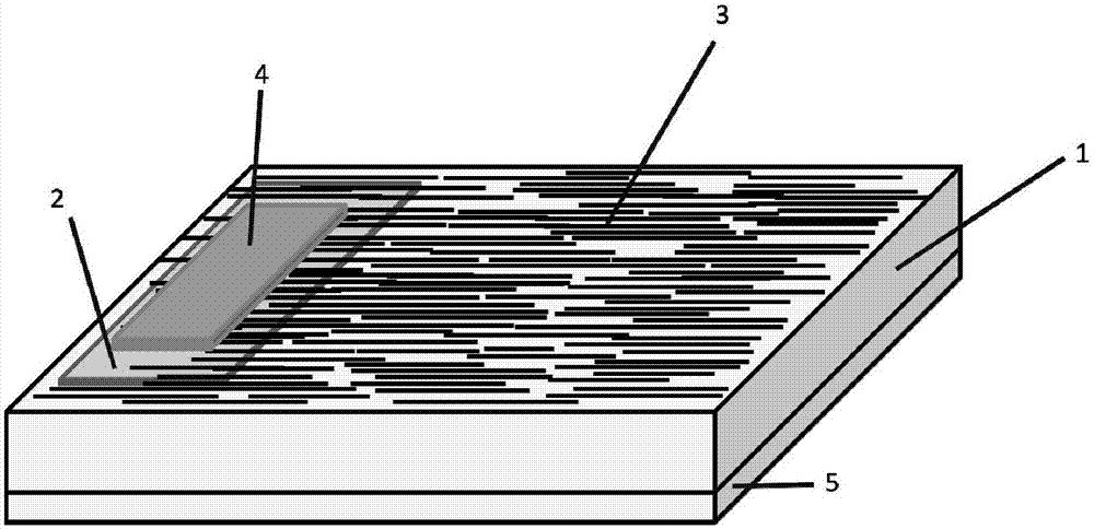
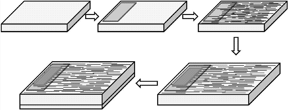
[0037] see figure 1 , the self-driven near-infrared photodetector of the present invention is based on a plane silicon 1, and an insulating region 2 is constructed at a local position on the upper surface of the plane silicon 1; 7 S 4 Quasi-one-dimensional nanostructures of KCu assembled by LB technique 7 S 4 Monolayer 3; KCu 7 S 4 The single-layer film 3 is partially located on the insulating region 2, and the remaining part is directly in contact with the upper surface of the planar silicon to form Si / KCu 7 S 4 Heterojunction; in KCu 7 S 4 A first metal thin film electrode 4 is deposited above the monolayer film 3, and KCu 7 S 4 The single-layer film 3 forms an ohmic contact; the first metal thin film electrode 4 is located above the insulating area 2 and does not exceed the area where the insulating area 2 is located; a second metal thin film electrode 5 is brushed on the back of the plane silicon 1 to form with the silicon Ohmic contact.

[0038] Specifically: i...

Embodiment 2

[0055] The self-driven near-infrared photodetector and the preparation method thereof in this embodiment are the same as those in Embodiment 1, except that the surface pressure in step D is 5 mN / m.

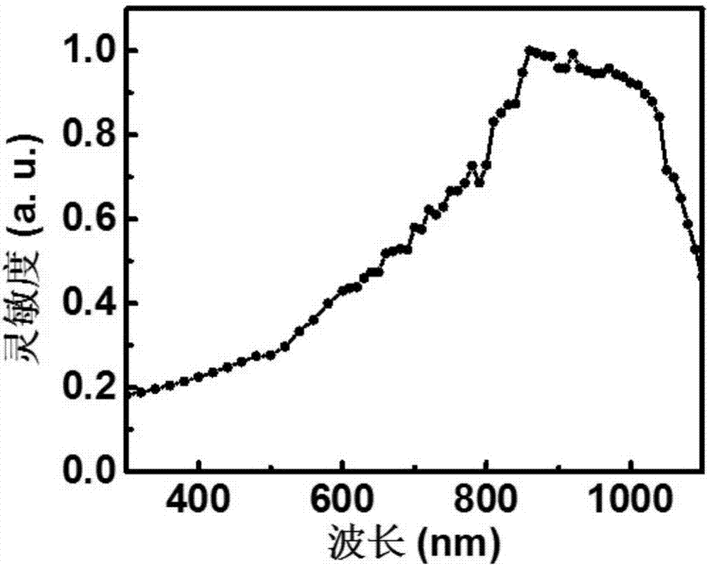
[0056] The self-driven near-infrared photodetector prepared in this example has a light intensity of 300 μW cm -2 , Under the irradiation of monochromatic light with a wavelength of 980nm, it exhibits remarkable photovoltaic characteristics, such as Figure 9 As shown, the open circuit voltage is 0.117V, the short circuit current is 3.27nA, and the fill factor is 16.91%.

Embodiment 3

[0058] The self-driven near-infrared photodetector and the preparation method thereof in this embodiment are the same as those in Embodiment 1, except that the surface pressure in step D is 15 mN / m.

[0059] The self-driven near-infrared photodetector prepared in this example has a light intensity of 300 μW cm -2 , Under the irradiation of monochromatic light with a wavelength of 980nm, it exhibits remarkable photovoltaic characteristics, such as Figure 10 As shown, the open circuit voltage is 0.064V, the short circuit current is 299nA, and the fill factor is 23.52%.


PUM

PropertyMeasurementUnit
electrical resistivityaaaaaaaaaa
thicknessaaaaaaaaaa

Abstract

The invention discloses a self-driven near infrared photodetector based on a potassium sulfate quasi-one-dimensional nanostructure and a preparation method thereof. The method comprises the steps that a KCu7S4 monolayer film assembled by a KCu7S4 quasi-one-dimensional nanostructure through an LB technology is transferred to an n-type silicon substrate on which an insulating region is constructed; the KCu7S4 monolayer film contacts the silicon substrate to form a Si/KCu7S4 heterojunction; a first metal thin film electrode in ohmic contact with the KCu7S4 monolayer film is deposited on the insulating region; and a second metal thin film electrode in ohmic contact with silicon is prepared on the back of the silicon substrate, and the self-driven near infrared photodetector is acquired. The self-driven near infrared photodetector provided by the invention has the advantages of simple preparation process, superior device performance and good compatibility with the existing semiconductor technology.

Description

technical field [0001] The invention relates to a self-driven near-infrared photoelectric detector and a preparation method thereof, in particular to a self-driven near-infrared photoelectric detector based on a copper potassium sulfate quasi-one-dimensional nanostructure and a preparation method thereof. Background technique [0002] Photodetectors are semiconductor devices that convert optical signals into electrical signals. The wavelength range that the human eye can perceive is 380-780nm, and there is a large amount of infrared light in daily life, so the photodetector can also be considered as an effective extension of the human eye. The penetration ability of mid- and far-infrared light (3-14μm) is strong, so it is widely used in the military field, and has important applications in infrared reconnaissance, infrared guidance, infrared night vision, infrared stealth and so on. For example, the U.S. Army Research Laboratory cooperated with Rockwell Scientific Corporati...

Claims


Application Information

Patent Timeline
Patent Type & Authority Applications(China)
IPC IPC(8): H01L31/109H01L31/0336H01L31/18
CPCH01L31/0336H01L31/109H01L31/18
Inventor 吴春艳王友义徐际宇吴亚东陆杨
Owner 合肥庐阳科技创新集团有限公司
Why Eureka
Try Eureka