Floating source field plate and floating drain field plate-based vertical type heterojunction field effect device

A heterojunction field effect and source field plate technology, which is applied in the field of microelectronics, can solve the problems that the field plate structure cannot effectively modulate the electric field distribution in the device, device failure, and current blocking layer failure.

Active Publication Date: 2017-09-15
XIDIAN UNIV
View PDF6 Cites 2 Cited by
  • Summary
  • Abstract
  • Description
  • Claims
  • Application Information

AI Technical Summary

Problems solved by technology

However, up to now, there is still no precedent of the field plate structure being successfully applied to GaN-based current aperture heterojunction field effect devices at home and abroad. This is mainly due to the inherent defects in the structure of GaN-based current aperture heterojunction field effect devices. As a result, the strongest electric field peak in the device drift layer is located near the interface between the current blocking layer and the aperture layer, and the electric field peak is far away from the surfaces on both sides of the drift layer, so the field plate structure can hardly play the role of effectively modulating the electric field distribution in the device, even in GaN The field plate structure is used in the base current aperture heterojunction field effect device, and there is almost no improvement in device performance
[0008] In addition, the existing GaN-based current aperture heterojunction field effect devices all use ohmic drains. When a very low reverse voltage is applied to the device drain, the current blocking layer in the device will fail, forming a large drain-source Leakage current, and as the drain reverse voltage increases, the device gate will also open forward, and a large gate current will pass, eventually leading to device failure
Therefore, none of the existing GaN-based current aperture heterojunction field effect devices can realize the reverse blocking function. break feature has no effect

Method used


Image

  • Floating source field plate and floating drain field plate-based vertical type heterojunction field effect device
  • Floating source field plate and floating drain field plate-based vertical type heterojunction field effect device
  • Floating source field plate and floating drain field plate-based vertical type heterojunction field effect device

Examples


Embodiment 1

[0094] Embodiment 1: making passivation layer is SiO 2 , and a vertical heterojunction field effect device based on floating source field plates and floating drain field plates with two drain floating field plates and two source floating field plates.

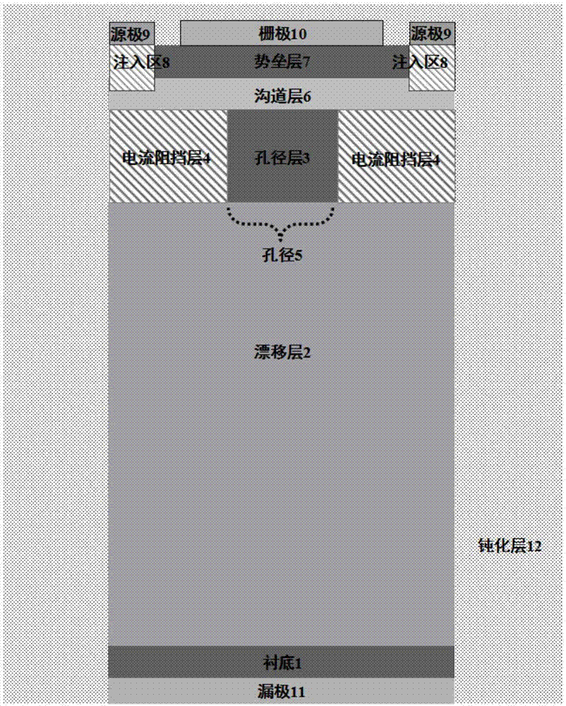
[0095] Step 1. Make drift layer 2 and aperture layer 3, such as image 3 a.

[0096] 1a) Use n - Type GaN material is used as the substrate 1, and the epitaxial doping concentration on the substrate 1 is 1×10 by using metal-organic chemical vapor deposition technology. 15 cm -3 the n - type GaN semiconductor material to form a drift layer 2, wherein:

[0097] The process conditions used for epitaxy are: the temperature is 950°C, the pressure is 40Torr, and the SiH 4 As the doping source, the flow rate of hydrogen gas is 4000 sccm, the flow rate of ammonia gas is 4000 sccm, and the flow rate of gallium source is 100 μmol / min;

[0098] 1b) Using metal-organic chemical vapor deposition technology, the epitaxial thickness on...

Embodiment 2

[0166] Embodiment 2: Making the passivation layer is SiO 2 , and a vertical heterojunction field effect device based on floating source field plates and floating drain field plates with two drain floating field plates and three source floating field plates.

[0167] The first step. Make drift layer 2 and aperture layer 3, such as image 3 a.

[0168] 1.1) Use n - Type GaN as the substrate 1; at a temperature of 950°C and a pressure of 40Torr, SiH 4 is the doping source, the flow rate of hydrogen gas is 4000 sccm, the flow rate of ammonia gas is 4000 sccm, and the flow rate of gallium source is 100 μmol / min, and the epitaxial doping concentration on the substrate 1 is 6×10 16 cm -3 the n - type GaN semiconductor material to form a drift layer 2;

[0169] 1.2) At a temperature of 950°C and a pressure of 40Torr, SiH 4 is the dopant source, the flow rate of hydrogen gas is 4000 sccm, the flow rate of ammonia gas is 4000 sccm, and the flow rate of gallium source is 100 μmol / ...

Embodiment 3

[0236] Example 3: The vertical heterojunction field effect based on the floating source field plate and the floating drain field plate with a passivation layer of SiN and one drain floating field plate and two source floating field plates device.

[0237] Step A. Make drift layer 2 and aperture layer 3, such as image 3 a.

[0238] A1) The temperature is 950°C, the pressure is 40Torr, and SiH 4 As the doping source, the flow rate of hydrogen gas is 4000 sccm, the flow rate of ammonia gas is 4000 sccm, and the flow rate of gallium source is 100 μmol / min. - Type GaN is used as the substrate 1, and the epitaxial doping concentration on the substrate is 1×10 by metal-organic chemical vapor deposition technology. 18 cm -3 the n - type GaN material to make the drift layer 2.

[0239] A2) The temperature is 950°C, the pressure is 40Torr, and SiH 4 is the dopant source, the flow rate of hydrogen gas is 4000 sccm, the flow rate of ammonia gas is 4000 sccm, and the flow rate of g...


PUM


Abstract

The invention discloses a floating source field plate and floating drain field plate-based vertical type heterojunction field effect device. The heterojunction field effect device comprises a schottky drain (11), a substrate (1), a drifting layer (2), an aperture layer (3), two symmetrical current blocking layers (4), a channel layer (6), a barrier layer (7) and a gate (10) from the bottom up; an aperture (5) is formed between the two current blocking layers (4); two sources (9) are deposited on the two sides of the barrier layer; injection regions (8) are arranged below the sources; all regions, except the schottky drain bottom, are covered with a passivation layer (14); the device is characterized in that a floating drain field plate (12) is manufactured on the inner lower part of the passivation layer on the two sides, and a floating source field plate (13) is manufactured on the upper part; and the current blocking layers adopt a two-stage-step structure. The heterojunction field effect device has the advantages of high breakdown voltage, simple process, low conduction resistance and high rate of finished products, and can be used for a power electronic system.

Description

technical field [0001] The invention belongs to the technical field of microelectronics and relates to a semiconductor device, in particular a vertical heterojunction field effect device based on a floating source field plate and a floating drain field plate, which can be used in a power electronic system. technical background [0002] Power semiconductor devices are the core components of power electronics technology. As energy and environmental issues become increasingly prominent, research and development of new high-performance, low-loss power devices has become one of the effective ways to improve power utilization, save energy, and alleviate energy crises. In the research of power devices, there is a serious restrictive relationship between high speed, high voltage and low on-resistance. Reasonable and effective improvement of this restrictive relationship is the key to improving the overall performance of the device. With the development of microelectronics technology...

Claims


Application Information

Patent Timeline
Patent Type & Authority Applications(China)
IPC IPC(8): H01L29/778H01L29/06H01L29/40
CPCH01L29/0611H01L29/0619H01L29/404H01L29/7786
Inventor 毛维石朋毫杜鸣郝跃张进成
Owner XIDIAN UNIV
Why Eureka
Try Eureka