Nonreciprocal spin-wave heterojunction waveguide material and preparation method and application thereof

A heterojunction, spin wave technology, applied in the direction of waveguide, material selection, waveguide type devices, etc., can solve the problems of difficult to change, the non-reciprocity of spin wave transmission is not obvious, and achieve a wide range of applications. Effect

Inactive Publication Date: 2017-09-22
UNIV OF ELECTRONICS SCI & TECH OF CHINA
View PDF12 Cites 9 Cited by
  • Summary
  • Abstract
  • Description
  • Claims
  • Application Information

AI Technical Summary

Problems solved by technology

However, it is difficult to change the "environment" of spin wave transmission on the upper and lower surfaces of a single-layer YIG film. The non-re

Method used


Image

  • Nonreciprocal spin-wave heterojunction waveguide material and preparation method and application thereof
  • Nonreciprocal spin-wave heterojunction waveguide material and preparation method and application thereof

Examples


Embodiment 1

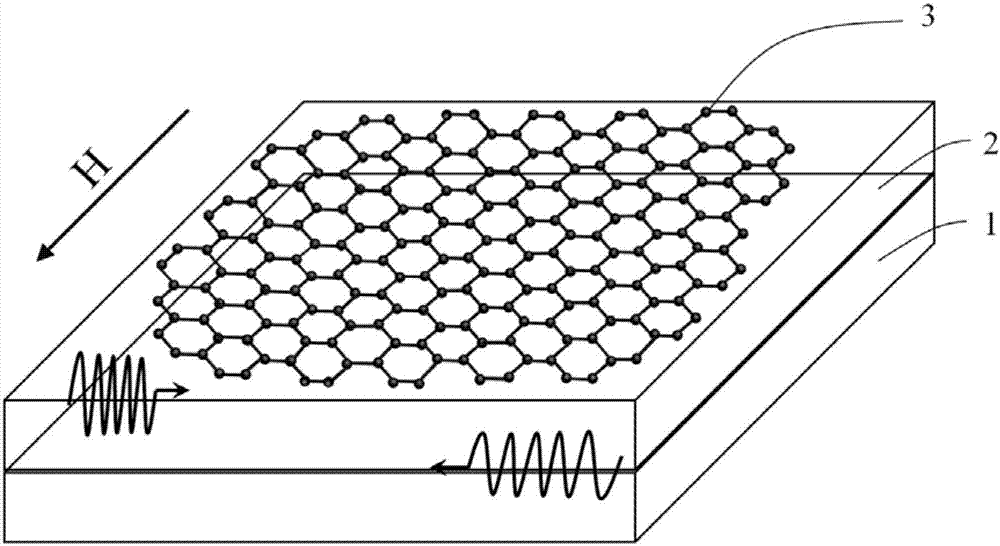
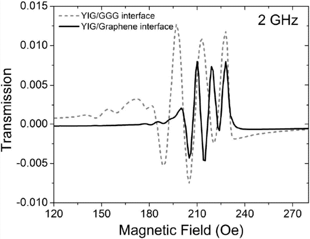
[0030] A non-reciprocal spin wave heterojunction waveguide material, which includes GGG (gadolinium gallium garnet) single crystal substrate and YIG / graphene heterojunction material, grown on the GGG single crystal substrate by liquid phase epitaxy High-quality YIG film, on the YIG film, transfer the single-layer graphene grown by the chemical vapor deposition method to the high-quality YIG film, and dry it to form a YIG / graphene heterojunction material. The YIG (yttrium iron pomegranate Stone) thin film is single crystal thin film, and thickness is at 100 nanometers, and described single-layer graphene utilizes vapor phase deposition method to grow and obtains, and described YIG / graphene heterojunction material maximum diameter is 3 inches.

[0031] The preparation method of above material, comprises the following steps:

[0032] S1: Choose high purity (higher than 99.99%) Fe 2 o 3 and Y 2 o 3 As a raw material, a high-quality YIG thin film is grown on a GGG single crysta...

Embodiment 2

[0038] A non-reciprocal spin-wave heterojunction waveguide material, which includes a GGG (gadolinium gallium garnet) single crystal substrate and a YIG / graphene heterojunction material, is deposited on a GGG single crystal using pulsed laser deposition (PLD) Growth high-quality YIG thin film on the substrate, on the YIG thin film, the single-layer graphene that vapor deposition method is grown is transferred on the high-quality YIG thin film, drying treatment forms YIG / graphene heterojunction material, described YIG (yttrium (yttrium) Iron garnet) film is a single crystal film with a thickness of 500 nanometers. The single-layer graphene is grown by vapor deposition method, and the maximum diameter of the YIG / graphene heterojunction material is 3 inches.

[0039] The preparation method of above material, comprises the following steps:

[0040] S1: Choose high purity (higher than 99.99%) Fe 2 o 3 and Y 2 o 3 As a raw material, Y was prepared by a solid-state reaction metho...

Embodiment 3

[0046] A non-reciprocal spin wave heterojunction waveguide material, which includes a GGG (gadolinium gallium garnet) single crystal substrate and a YIG / graphene heterojunction material, which is deposited on the GGG single crystal substrate by magnetron sputtering Growth high-quality YIG thin film, on YIG thin film, the monolayer graphene that gas phase deposition method is grown is transferred on the high-quality YIG thin film, drying treatment forms YIG / graphene heterojunction material, described YIG (yttrium iron pomegranate (Si) film is a monocrystalline film with a thickness of 1 micron. The single-layer graphene is grown by vapor deposition, and the area of ​​the YIG / graphene heterojunction material is 5×5cm 2 .

[0047] The preparation method of above material, comprises the following steps:

[0048] S1: Choose high purity (higher than 99.99%) Fe 2 o 3 and Y 2 o 3 As a raw material, Y was prepared by a solid-state reaction method 3 Fe 5 o 12 The target materia...


PUM

PropertyMeasurementUnit
Thicknessaaaaaaaaaa
Thicknessaaaaaaaaaa

Abstract

A nonreciprocal spin-wave heterojunction waveguide material comprises a GGG (gadolinium gallium garnet) monocrystalline substrate and a YIG (yttrium iron garnet)/graphene heterojunction material; the YIG/graphene heterojunction material is formed by growing YIG film on the surface of the GGG monocrystalline substrate, transferring single-layer graphene to the YIG film, and drying. The invention also provides a preparation method and application of the nonreciprocal spin-wave heterojunction waveguide material. Compared with single YIG film, the YIG/graphene heterojunction film prepared herein has the advantage that spin waves propagated on the upper and lower surfaces are of significant nonreciprocity, namely both amplitude and peaks of the spin waves propagated on the upper and lower surfaces of the YIG/graphene heterojunction material experience significant changes.

Description

technical field [0001] The invention relates to the technical field of new materials, in particular to a non-reciprocal spin wave heterojunction waveguide material and its preparation method and application. Background technique [0002] With the rapid development of information technology, the miniaturization and low power consumption of traditional electronic devices are facing severe bottlenecks due to the existence of current Joule heat. Spin Waves (Spin Waves) is the collective propagation process of electron spin precession in magnetically ordered materials, with no heat dissipation, non-ohmic contact, extremely high operating frequency range, room temperature Bose-Einstein condensation, Macroscopic quantum effects such as magnon superfluidity, etc. Information transmission and logic calculation based on spin waves may become one of the important ways of information transmission and processing in the post-Moore era. The waveguide material of the spin wave requires lo...

Claims


Application Information

Patent Timeline
IPC IPC(8): C30B29/24C30B19/00C30B29/02C30B25/02H01L43/10H01P3/00H01Q1/38
CPCH01P3/00H01Q1/38C30B19/00C30B25/02C30B29/02C30B29/24H10N50/85
Inventor 金立川洪彩云张怀武饶毅恒杨青慧钟智勇文岐业
Owner UNIV OF ELECTRONICS SCI & TECH OF CHINA
Why Eureka
Try Eureka