Processing technology for forming micro-nano multi-layer composite structure on metal surface

A metal surface and composite structure technology, applied in metal processing equipment, manufacturing tools, welding equipment, etc., can solve the problems of high price, difficulty in industrial application, difficulty in controllability of micro-nano structure, etc., and achieve good ductility and flexibility , Excellent thermal fatigue resistance, not easy to stress concentration effect

Active Publication Date: 2017-10-17
UNIV OF SCI & TECH OF CHINA
View PDF7 Cites 1 Cited by
  • Summary
  • Abstract
  • Description
  • Claims
  • Application Information

AI Technical Summary

Problems solved by technology

The survey found that the above-mentioned technologies can handle small areas, but there are still great difficulties in large-area industrial applications, and the price is expensive
In comparison, sintering has certain advantages in large-area applications, but sintering requires strict process conditions, and there are great difficulties in the contr...

Method used


Image

  • Processing technology for forming micro-nano multi-layer composite structure on metal surface
  • Processing technology for forming micro-nano multi-layer composite structure on metal surface
  • Processing technology for forming micro-nano multi-layer composite structure on metal surface

Examples


Embodiment 1

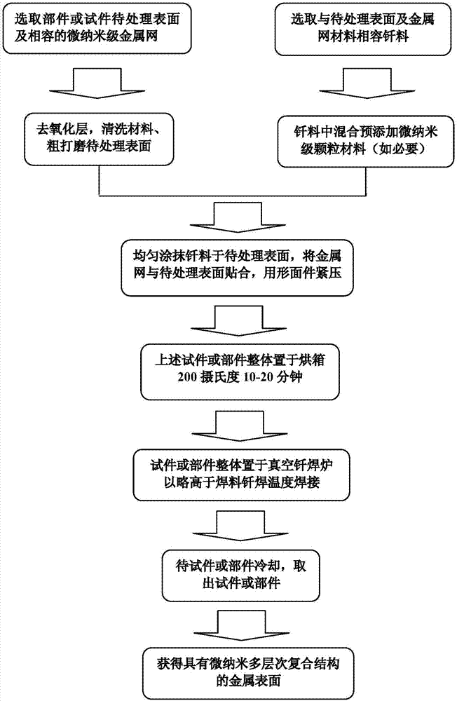
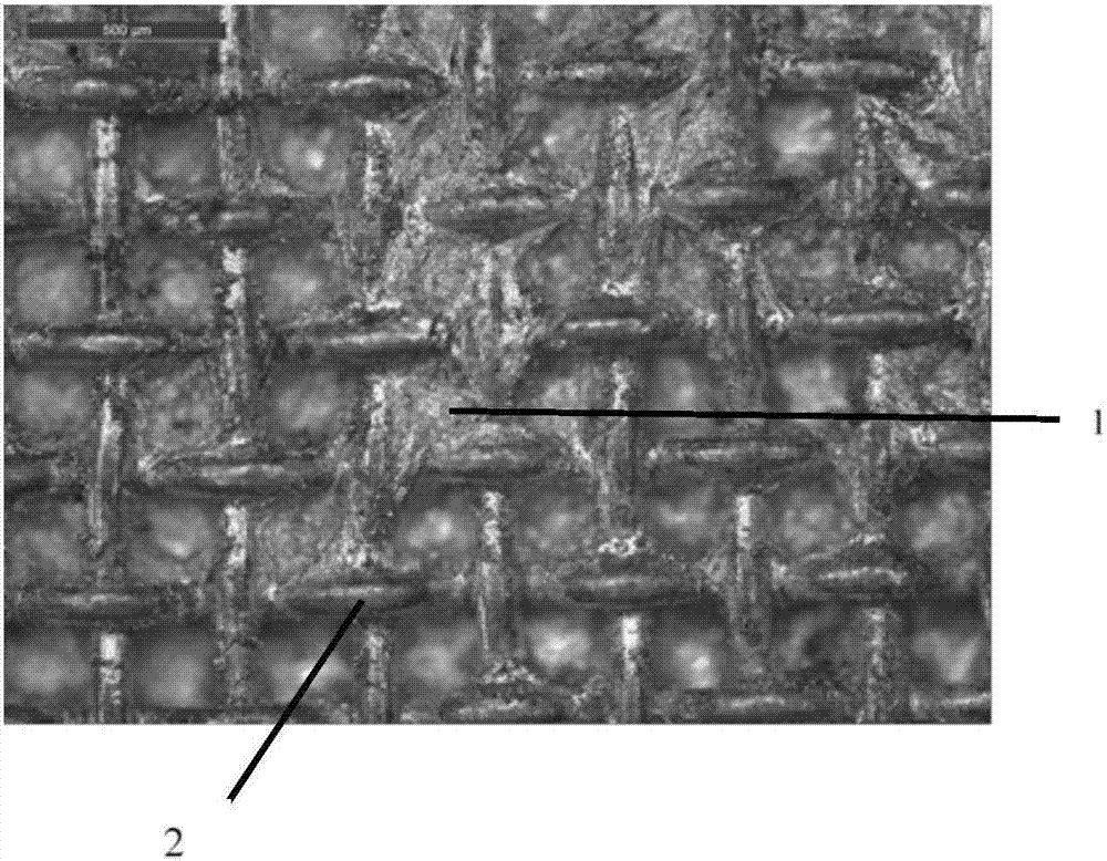
[0034] (1) Select chromium-zirconium copper of 100*10*10mm, of which the surface of 100*10mm is the surface to be treated, and prepare a micron-sized porous copper mesh corresponding to the size of the surface to be treated, that is, 100*10mm, and its wire diameter is 100μm , porosity 250μm, and silver-copper-titanium solder;

[0035] (2) And treat the surface of chrome-zirconium-copper, roughen the surface first, apply dilute hydrochloric acid on the surface to be treated for deoxidation treatment, and then use alcohol and water to clean;

[0036] (3) Cut the copper mesh with the same size as the chrome-zirconium copper surface to be treated, that is, the size is 100*10mm micron-scale pores, so that the copper mesh can be pressed flat and can fit the surface to be treated, and ensure that it can be well attached to the surface to be treated combine;

[0037] (4) Use dilute hydrochloric acid to clean the chrome-zirconium-copper surface to be treated and the copper mesh to rem...

Embodiment 2

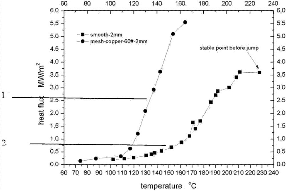
[0046] (1) Select chromium-zirconium copper of 100*10*10mm, of which the surface of 100*10mm is the surface to be treated, and prepare a micron-sized porous copper mesh corresponding to the size of the surface to be treated, that is, 100*10mm, and its wire diameter is 60μm , Pore 125μm, and silver-copper-titanium solder;

[0047] (2) And treat the surface of chrome-zirconium-copper, first roughen the surface, apply dilute hydrochloric acid on the surface to be treated for deoxidation treatment, and then use alcohol and water to clean;

[0048] (3) Cut the copper mesh that is consistent with the size of the chrome-zirconium copper surface to be treated, that is, the size is 100*10mm, the wire diameter is 60 μm, and the pores are 125 μm. Good adhesion to the surface to be treated;

[0049] (4) Use dilute hydrochloric acid to clean the chrome-zirconium-copper surface to be treated and the copper mesh to remove the oxide layer, then use alcohol to clean again, and dry;

[0050] ...

Embodiment 3

[0056] (1) Corresponding to the size of the surface to be treated, that is, a micron-scale porous copper mesh with a size of 100*10mm, its wire diameter is 100 μm, the pores are 250 μm, silver-copper-titanium solder, and nano-diamond powder with particles of 100 nm;

[0057] (2) And treat the surface of chrome-zirconium-copper, roughen the surface first, apply dilute hydrochloric acid on the surface to be treated for deoxidation treatment, and then use alcohol and water to clean;

[0058] (3) Cut the copper mesh with the size of the chrome-zirconium copper surface to be treated, that is, the size is 100*10mm, the wire diameter is 100μm, and the pores are 250μm. Good adhesion to the surface to be treated;

[0059] (4) Use dilute hydrochloric acid to clean the chrome-zirconium-copper surface to be treated and the copper mesh to remove the oxide layer, then use alcohol to clean again, and dry;

[0060] (5) the nano-diamond powder of 100nm is mixed with silver-copper-titanium sol...


PUM

PropertyMeasurementUnit
Wire diameteraaaaaaaaaa
Porosityaaaaaaaaaa
Wire diameteraaaaaaaaaa

Abstract

The invention relates to a processing technology for forming micro-nano multi-layer composite structure on the metal surface. The processing technology is suitable for improving the supercooling boiling surface heat exchange performance and mainly applied to high heat flow parts which adopt liquid working medium supercooling boiling surface heat exchange such as fusion reactor first wall. The basic method comprises the following steps that according to practical parts or test parts, the metal surface to be disposed, corresponding micron grade pore metal nets and compatible brazing filler metal are selected, planishing is conducted on the metal surface to be disposed, oxide layer removing is conducted, and the selected brazing filler metal is painted evenly; then the metal surface is attached to the metal nets, and drying is conducted.; the metal nets and the metal surface to be disposed are pressed by profile objects, and vacuum brazing is conducted; and after finishing, a micro-nano multi-layer composite structure surface is obtained, the metal nets constitute micron grade convex-concave surface pores, and a surface after the brazing filler metal is melted and planes which is connected with metal wires present nano-grade holes and rough units. The processing technology has the characteristics that the controllability is high, the cost is low, the processing technology is simple and convenient, and the formed surface structure does not damage base materials.

Description

technical field [0001] The invention relates to a processing technology for forming a micro-nano multi-level composite structure on the surface of a metal (such as copper or other alloys), and belongs to the technical field of micro-nano processing of the material surface and the field of metal material surface modification treatment. Background technique [0002] Because materials with micro-nano surface structure have great variation compared with macroscopic properties in terms of sound, light, electromagnetic, thermodynamics, and chemical activity, and exhibit special properties different from macroscopic properties, people have been looking for comparisons. Convenient and efficient micro-nano processing method. [0003] Studies have found that heat transfer surfaces with micro-nano surface structures can greatly improve the performance of subcooled boiling heat transfer, which is of great significance to the development of industrial heat exchangers with strong heat tra...

Claims


Application Information

Patent Timeline
IPC IPC(8): B23K1/008B23K1/20
CPCB23K1/008B23K1/203B23K1/206
Inventor 黄生洪乐吴生
Owner UNIV OF SCI & TECH OF CHINA
Why Eureka
Try Eureka