Semiconductor bonding technology based on palladium copper wire

A bonding process and semiconductor technology, which is applied in the direction of semiconductor devices, semiconductor/solid-state device manufacturing, electric solid-state devices, etc., can solve the problems of narrow welding process parameters, complicated process, high difficulty, etc., and achieve a wide range of bonding process parameters, Eliminate oxidation problems and save costs

Active Publication Date: 2017-10-17
佛山市彩立德光电技术有限公司
View PDF4 Cites 4 Cited by
  • Summary
  • Abstract
  • Description
  • Claims
  • Application Information

AI Technical Summary

Problems solved by technology

Therefore, compared with gold wire, copper wire bonding has problems such as more co

Method used


Image

  • Semiconductor bonding technology based on palladium copper wire
  • Semiconductor bonding technology based on palladium copper wire
  • Semiconductor bonding technology based on palladium copper wire

Examples


Embodiment 1

[0047] A kind of semiconductor bonding process based on palladium copper wire that the present embodiment provides, it comprises:

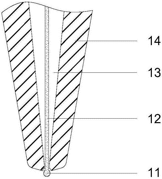
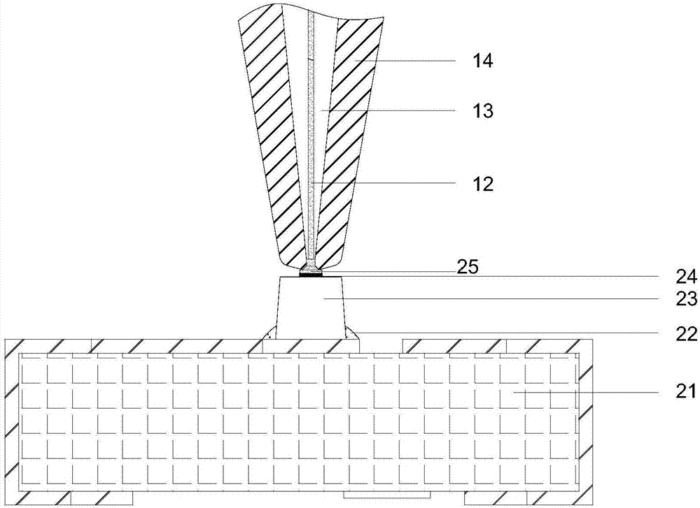
[0048] Step 1: Burn the ball, EFO (EFO, Electronic Flame Offs, the high-voltage electricity generated by the ignition box is transmitted to the tip of the ignition rod through the ignition cable, and the discharge between the exposed metal wire of the chopper forms a complete current loop .) Afterwards, burn-in balls 11 are formed (burn-in balls, FAB, Free Air Ball, that is, small balls formed by wire tail sintering after electronic ignition in the wire-bonding burn-in ball stage.) The size of burn-in balls 11 is 1.6-2.0 mil, where 11 is a pre-burned ball, 12 is a welding wire, 13 is a chopper cavity, and 14 is a chopper. See figure 1 .

[0049]Step 2: 1 welding (welding of the first welding point), the chopper 14 moves to the position of the pad 24 of the 1 welding chip, and under the action of the set power, pressure and temperature, the 1 wel...

Embodiment 2

[0054] A kind of semiconductor bonding process based on palladium copper wire that the present embodiment provides, it comprises:

[0055] Step 1: First make pre-planted balls 4 on the board pad 311 (the second soldering functional area 311) of the PCB 31, and set the size of the pre-fired balls to 1.8-2.2 mil. In this process, a uniform and thin copper-nickel-gold-palladium-copper IMC (board pad 311 is copper, nickel, and gold) or copper-nickel-silver-palladium-copper IMC (board pad 311 is copper, copper, and gold) is formed in the second welding functional area 311. Nickel, silver three layers), see Figure 6 .

[0056] Step 2: Burn the ball, EFO (EFO, Electronic Flame Offs, the high-voltage electricity generated by the ignition box is transmitted to the tip of the ignition rod through the ignition cable, and the discharge between the exposed metal wire of the chopper forms a complete current loop .) Afterwards, burn-in balls 11 are formed (burn-in balls, FAB, Free Air Bal...

Embodiment 3

[0071] See Figure 11 .

[0072] A semiconductor bonding process based on palladium copper wire, comprising:

[0073] A. Move the chopper to the position of the chip pad, and use a bonding wire composed of a palladium-plated pure copper wire to make the solder ball of the first solder joint;

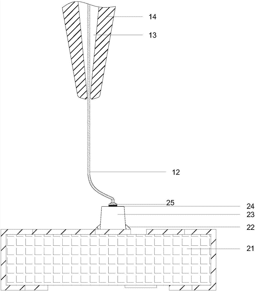
[0074] B. Pull the wire arc, the welding head drives the rivet to lift up, the welding wire is pulled to the set height, and then moves from the highest point to the second solder joint on the PCB board to complete the wiring of the welding wire;

[0075] C. Move the chopper to the position of the solder pad of the PCB board, and use the welding wire to weld the second solder joint;

[0076] Among them, when making the first solder joint and the second solder joint, use protective gas to fill the perimeter of the riving knife and the riving knife. The composition of the protective gas is: 95% to 99% nitrogen and 1% to 5% hydrogen, weight percentage.

[0077] 95-99% N 2 and 1 to 5% H...


PUM

PropertyMeasurementUnit
Thicknessaaaaaaaaaa
Thicknessaaaaaaaaaa
Thicknessaaaaaaaaaa

Abstract

The invention relates to a semiconductor bonding technology based on a palladium copper wire. The semiconductor bonding technology comprises steps that A, a cleaver is moved to a position of a chip pad, and a welding wire rod formed by a pure copper wire having a palladium-plated surface is used to produce a welded ball of a first welding point; B, a bank is pulled, and after the welding wire rod is pulled to a set height, the welding wire rod is moved to a position of a second welding point from the highest point, and the wiring of the welding wire rod is completed; C, the cleaver is moved to the position of the bonding pad of a PCB, and the welding wire rod is connected with the second welding point in a welded manner; during the production of the first welding point and the second welding point, the cleaver and the periphery of the cleaver are filled with protection gas, which comprises 95wt %-99wt % nitrogen and 1wt%-5wt% hydrogen. The price of the palladium copper wire is lower than 10% of a price of a gold wire, and therefore a lot of costs are saved. During the bonding process, the hydrogen is used as the protection gas, and the copper can be reduced from copper oxide. A bonding technological parameter range is widened, and the optimal technological parameter adjustment is facilitated, and therefore excellent bonding effect is acquired.

Description

technical field [0001] The invention relates to the technical field of semiconductor packaging, in particular to a semiconductor bonding process based on palladium-copper wires. Background technique [0002] At present, the packaging industry is still dominated by gold wire bonding, and gold wire bonding has always occupied a dominant position in the packaging process. With the price of packaging products going down, the price of gold wire has become an unbearable burden for the packaging industry, and reducing the cost of packaging is an urgent requirement of the market. [0003] In recent years, copper has quickly gained a solid position as an alternative material for gold wire bonding. Its advantages include higher electrical and thermal conductivity than gold, and less formation of IMC (Inter-metallic Compound, which refers to metal and Metals, metals and metalloids are combined in the form of metal bonds or covalent bonds), and have better mechanical stability. [000...

Claims


Application Information

Patent Timeline
IPC IPC(8): H01L21/60H05K3/34
CPCH01L24/45H01L24/85H05K3/3426H01L2224/45664H01L2224/4556H01L2224/45147H01L2224/85075H01L2224/85801H01L2224/78301H01L2224/85181H01L2224/92247H01L2224/32225H01L2224/48091H01L2224/48227H01L2224/48465H01L2224/73265H01L2924/00014H01L2924/00012H01L2924/00H01L2224/43848
Inventor 廖伟春
Owner 佛山市彩立德光电技术有限公司
Why Eureka
Try Eureka