Silicon carbide TrenchMOS device and manufacturing method thereof

A technology of silicon carbide and devices, which is applied in the field of silicon carbide TrenchMOS devices and its production, can solve the problems of high power loss, low work efficiency, and high production costs

Active Publication Date: 2017-10-17
HANGZHOU SILICON-MAGIC SEMICON TECH CO LTD
View PDF6 Cites 14 Cited by
  • Summary
  • Abstract
  • Description
  • Claims
  • Application Information

AI Technical Summary

Problems solved by technology

Using the silicon carbide Trench MOS device of the present invention in the above circuit can overcome the problems of high power loss, low work efficiency and high production cost in the prior art

Method used


Image

  • Silicon carbide TrenchMOS device and manufacturing method thereof
  • Silicon carbide TrenchMOS device and manufacturing method thereof
  • Silicon carbide TrenchMOS device and manufacturing method thereof

Examples


Embodiment 1

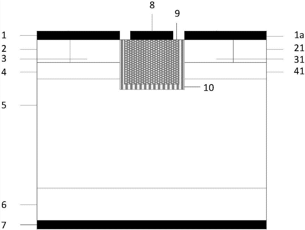
[0099] A silicon carbide Trench MOS device, its cell structure is as follows figure 2 Shown includes: metal drain electrodes 7, N + Substrate 6 and N - Epitaxial layer 5; characterized in that: the N - The two ends of the upper layer of the epitaxial layer 5 respectively have first P + polysilicon region 11 and the second P + polysilicon region 111, the first P + polysilicon region 11 and the second P + The upper surface of the polysilicon region 111 is respectively provided with a first metal electrode 12 and a second metal electrode 121; + N between the polysilicon regions 11, 111 - The epitaxial layer 5 has a Trench gate structure, and the Trench gate structure includes a polysilicon gate 9, a gate oxide layer 10 disposed on the bottom surface and sidewalls of the polysilicon gate 9, and a metal gate 8 disposed on the upper surface of the polysilicon gate 9; + N between the polysilicon region 11 and the Trench gate structure - The upper layer of the epitaxial layer ...

Embodiment 2

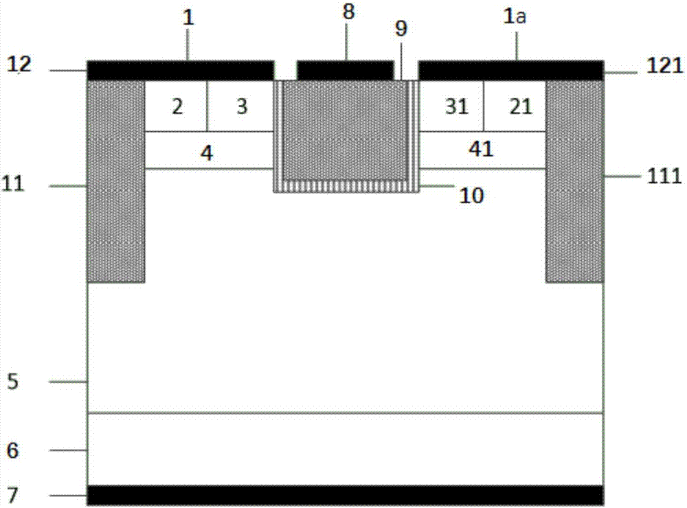
[0102] This implementation except in the first P + polysilicon region 11 and the second P + There is a first P in contact with the polysilicon region 111 below + SiC region 14 and the second P + SiC region 141; the P +The width of the silicon carbide region 14, 141 and P + The polysilicon region 11 has the same width, as image 3 shown.

[0103] The P added in this embodiment + The SiC region 14, 141 is able to P + The polysilicon regions 11, 111 and the trench gate play the role of electric field shielding, thereby improving the withstand voltage of the device, and have a certain effect on suppressing the reverse leakage current.

Embodiment 3

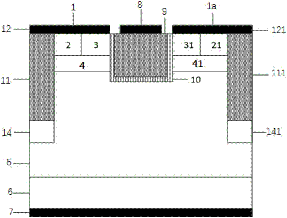
[0105] This implementation except in the first P + polysilicon region 11 and the second P + There is a first P in contact with the polysilicon region 111 below + SiC region 14 and the second P + SiC region 141; the P + The width of the silicon carbide region 14, 141 is greater than P + The width of the polysilicon region 11, such as Figure 4 As shown, in this implementation P + The width of the silicon carbide regions 14 and 141 ranges from 1.0 to 2.6 μm.

[0106] In this example, P + The silicon carbide regions 14, 141 have larger lateral dimensions (i.e., widths), which have a stronger electric field shielding effect on the P+ polysilicon regions 11, 111 and trench gates compared to Example 2, further improving the withstand voltage of the device, and at the same time The reverse leakage current is also further suppressed.


PUM

PropertyMeasurementUnit
thicknessaaaaaaaaaa
thicknessaaaaaaaaaa
thicknessaaaaaaaaaa

Abstract

The invention discloses a silicon carbide TrenchMOS device and manufacturing method thereof, belonging to the technical field of power semiconductors. Considering the defects of an external anti-parallel fast recovery diode (FRD) and a parasitic diode directly using a silicon carbide TrenchMOS device, a polysilicon area is additionally arranged in the p+ contact area of a conventional device, so that a Si/SiC heterojunction is formed by the polysilicon and silicon carbide epitaxial layer material, and furthermore, a diode is integrated in the device. The junction voltage drop is significantly reduced when a device diode is applied, and the conductive mode during the diode application is converted from bipolar conduction into single polar conduction, so that the silicon carbide TrenchMOS device has the advantages of short reverse recovery time and less reverse recovery charge. The device structure also has the advantages of low parasitic silicon carbide diode reverse leakage, high breakdown voltage and good device temperature stability. Therefore, the silicon carbide TrenchMOS device has wide prospects in circuits such as an inversion circuit and a chopper circuit.

Description

technical field [0001] The invention belongs to the technical field of power semiconductors, and in particular relates to a silicon carbide Trench MOS device and a manufacturing method thereof. Background technique [0002] Power devices and their modules provide an effective way to realize the conversion between various forms of electric energy, and have been widely used in national defense construction, transportation, industrial production, medical and health and other fields. Since the first power device application in the 1950s, each generation of power devices has enabled more efficient conversion and use of energy. Therefore, the history of power semiconductor devices, that is, the history of new power semiconductor devices. [0003] Traditional power devices and modules are dominated by silicon-based power devices, mainly thyristors, power PIN devices, power bipolar junction devices, power MOSFETs, and insulated gate field-effect transistors, and have been obtained ...

Claims


Application Information

Patent Timeline
Patent Type & Authority Applications(China)
IPC IPC(8): H01L27/06H01L29/24H01L29/423H01L21/336H01L29/78
CPCH01L27/0629H01L29/24H01L29/42356H01L29/66068H01L29/78
Inventor 张金平邹华刘竞秀李泽宏任敏张波
Owner HANGZHOU SILICON-MAGIC SEMICON TECH CO LTD
Why Eureka
Try Eureka