Preparation method of graphene composite film with conducting circuit on surface

A graphene composite and graphene film technology, applied to the conductive layer on the insulating carrier, etc., can solve the problems that the graphene film is damaged, easy to fall off, unsuitable for flexible electronic and electrical applications, etc.

Active Publication Date: 2017-10-27
宁波柔碳电子科技有限公司
View PDF5 Cites 3 Cited by
  • Summary
  • Abstract
  • Description
  • Claims
  • Application Information

AI Technical Summary

Problems solved by technology

However, this method has the following disadvantages: 1. There are many process steps, which may cause damage to the graphene film during the process of printing conductive silver paste
3. The chemical activity of the graphene surface is low, the bonding force between the conductive silver paste and the graphene film is weak, and it is easy to fall off
4. The electrode formed after the conductive silver paste is cured is not flexible, and it is easy to crack and damage after bending, which is not suitable for the application of flexible electronic and electrical fields

Method used


Image

  • Preparation method of graphene composite film with conducting circuit on surface
  • Preparation method of graphene composite film with conducting circuit on surface
  • Preparation method of graphene composite film with conducting circuit on surface

Examples


preparation example Construction

[0034] The invention provides a kind of preparation method of the graphene composite film with conductive circuit, comprises the following steps:

[0035] 1) forming a conductive line on the surface of the first substrate to obtain a substrate material;

[0036] 2) Obtaining the above-mentioned steps on the surface with conductive lines of the substrate material, compounding one or more layers of graphene film, and then combining the second substrate on the surface of the graphene film to obtain an intermediate product;

[0037] 3) Removing the first substrate of the intermediate product by chemical etching to obtain a graphene composite film with conductive lines.

[0038] In the present invention, firstly, conductive lines are formed on the surface of the first substrate to obtain the substrate material.

[0039] In the present invention, the material of the first substrate is not particularly limited, and the material of the substrate well-known to those skilled in the art...

Embodiment 1

[0075] a. Nickel electroplating is used to form the circuit shape on the copper foil.

[0076] Combine copper foil with plastic mask. The required circuit shape is hollowed out on the plastic mask. Put the copper foil / plastic mask into the electroplating solution, pass through the current, and form a nickel circuit of the desired shape on the copper foil. The numerical value of the passing current is 0.1-10A.

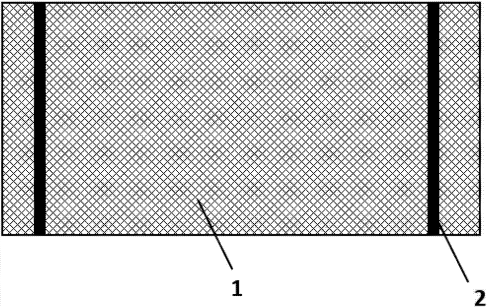
[0077] see figure 1 , figure 1 It is a schematic top view structure diagram of the product formed in step a of Example 1 of the present invention. Wherein, 1 is the first substrate, and 2 is a highly conductive pattern (conductive circuit).

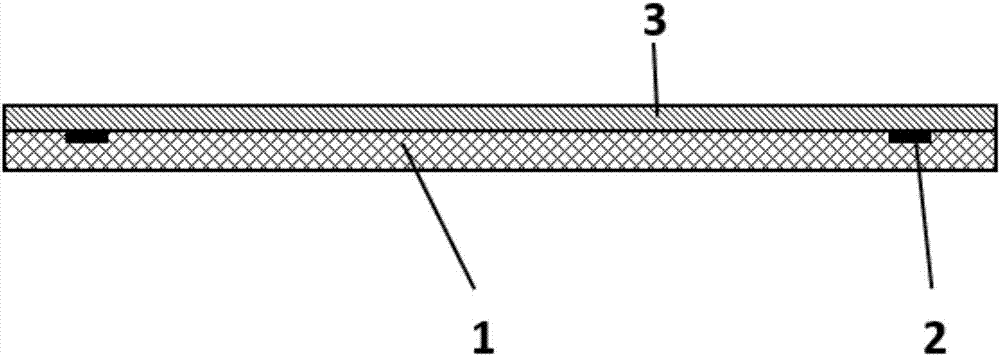
[0078] b. A graphene film is grown on the surface of the copper foil by chemical vapor deposition.

[0079] Put the copper foil into the chemical vapor deposition equipment, evacuate and heat up to the growth temperature of 1000±50°C, and inject methane to obtain the graphene film.

[0080] see figure 2 , figure 2 It is ...

Embodiment 2

[0089] a. Nickel electroplating is used to form the circuit shape on the copper foil.

[0090] Combine copper foil and glass mask. The desired circuit shape is hollowed out on the glass mask. Put the copper foil / glass mask into the electroplating solution, pass through the current, and form a nickel circuit of the desired shape on the copper foil. The numerical value of the passing current was 5A.

[0091] b. A graphene film is grown on the surface of the copper foil by chemical vapor deposition.

[0092] Put the copper foil into the chemical vapor deposition equipment, evacuate and heat up to the growth temperature of 1000±50°C, and feed ethylene to obtain the graphene film.

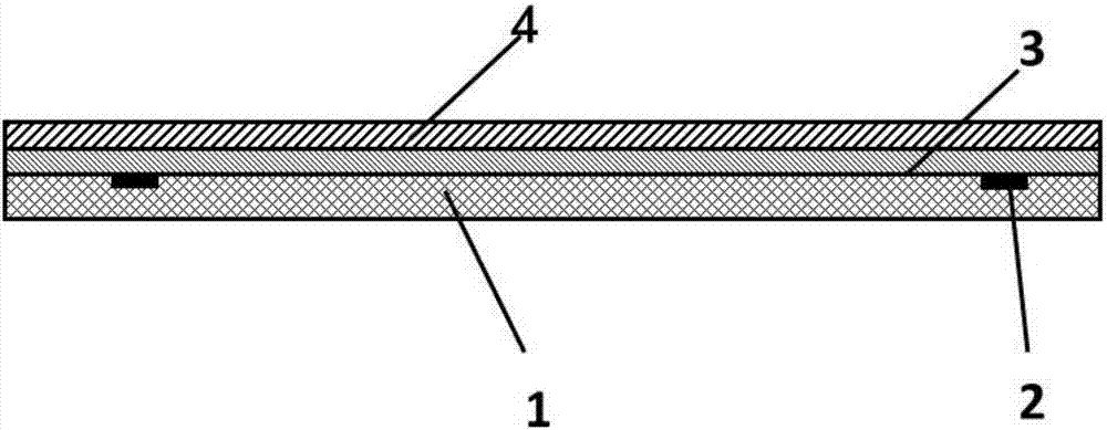
[0093] c. Then bond the graphene film surface of the copper foil to the PEN transparent substrate with hot melt adhesive.

[0094] d. Then put the bonded transparent substrate, graphene and copper foil into the etching solution. The etching solution is composed of a mixed solution of copper sulfate ...


PUM

PropertyMeasurementUnit
thicknessaaaaaaaaaa
thicknessaaaaaaaaaa
widthaaaaaaaaaa

Abstract

The invention provides a preparation method of a graphene composite film with a conducting circuit on a surface. The preparation method comprises the following steps: firstly forming a conducting circuit on the surface of a first substrate to obtain the substrate material; compounding a layer or multi-layer graphene film on the surface with the conducting circuit of the substrate material obtained in above-mentioned step, and then combining a second substrate on the surface of the graphene film to obtain an intermediate product; finally removing the first substrate of the above-mentioned intermediate product by using the chemical etching method to obtain the graphene composite film with the conducting circuit. A high-conducting patter can be formed on the graphene film surface by using the preparation method disclosed by the invention, and the shape of the formed high-conducting pattern is random, especially, the binding force between the conducting circuit and the graphene film is good, and the high-conducting pattern has the good flexibility. Meanwhile, the preparation method provided by the invention is not only simple and practicable in process procedure, but also can match with the process procedure of the graphene film, and is suitable for the large-scale industrial application.

Description

technical field [0001] The invention belongs to the technical field of graphene composite films, and relates to a preparation method of a graphene composite film with conductive lines, in particular to a preparation method of a graphene composite film with conductive lines on the surface. Background technique [0002] Graphene is a new material with a single-layer sheet structure composed of carbon atoms. It is a planar film composed of carbon atoms with sp2 hybrid orbitals forming a hexagonal honeycomb lattice, a two-dimensional material with a thickness of only one carbon atom. As a two-dimensional crystal composed of carbon atoms with only one layer of atomic thickness, it is the thinnest material and the strongest material currently in the application field, and its fracture strength is 200 times higher than that of steel, and it is also very good Excellent elasticity, the stretching range can reach 20% of its own size; at the same time, graphene has a huge theoretical ...

Claims


Application Information

Patent Timeline
Patent Type & Authority Applications(China)
IPC IPC(8): H01B5/14
CPCH01B5/14
Inventor 白晓航汪伟刘兆平
Owner 宁波柔碳电子科技有限公司
Why Eureka
Try Eureka