Thin film and switch material for phase change memory chip, and preparation method of switch material

A phase-change memory and switching material technology, applied in electrical components and other directions, can solve the problems of difficult commercial production, increased complexity of PCM chip device processing and preparation processes, and low yield, and achieve improved productivity, yield, and electrical conductivity. The effect of improving, increasing productivity and efficiency

Active Publication Date: 2017-10-27
PIONEER MATERIALS INC CHENGDU
View PDF6 Cites 5 Cited by
  • Summary
  • Abstract
  • Description
  • Claims
  • Application Information

AI Technical Summary

Problems solved by technology

[0004] However, there are many shortcomings in the existing switch materials, which lead to the increase in the complexity of the processing and preparation process for deep processing to prepare PCM chip devices, and it is difficult to carry out large-scale commercial production, or in other words, when using these switch materials to manufacture PCM chips , its yield is quite low

Method used


Image

  • Thin film and switch material for phase change memory chip, and preparation method of switch material
  • Thin film and switch material for phase change memory chip, and preparation method of switch material
  • Thin film and switch material for phase change memory chip, and preparation method of switch material

Examples


preparation example Construction

[0044] The present invention also provides a preparation method of the switch material for the phase change memory chip. The preparation method comprises: powder-making, hot-pressing sintering and cooling of the mixture under vacuum conditions, and the mixture contains mixed chalcogen compounds and carbon nanotubes.

[0045] Further, as an optional solution, in the mixture, the chalcogen compound and the carbon nanotubes are mixed in the form of powder. Preferably, the powdered elemental sulfur compound is obtained by grinding in a protective gas (such as nitrogen+hydrogen) environment.

[0046] As an optional implementation, the method for preparing the mixture may be: ball milling the chalcogen compound in a closed environment of protective gas (non-oxidizing atmosphere, such as nitrogen + hydrogen) to prepare the first powder. Then, fill it with argon to normal pressure, add carbon nanotubes and continue ball milling. The size of the crushed chalcogen compound doped with ...
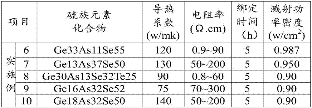
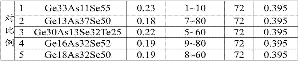
Embodiment 1

[0062] A switch material for phase-change memory chips. It is formed by doping 5 at % carbon nanotubes in a ternary chalcogen compound of Ge, As, Se. Among them, the ternary chalcogen compound is Ge33As12Se55, its thermal conductivity is 0.23W / mk, and its resistivity is 10 3 ~10 4 (Ω.cm). The switching material after carbon nanotube doping is Ge31.4As11.4Se52.2CNT5. CNT is a single-walled carbon nanotube with an inner diameter of 5nm and a length of about 2000nm, and its type is an electrical conductor. Its preparation method is as follows: the ternary chalcogen compound and carbon nanotubes are ball-milled into powder in a closed environment of protective gas atmosphere, and the powder is put into a graphite mold, and then in the graphite mold, 1.0×10 -3 Under the vacuum degree of Pa, sinter at 280°C and 400 tons of pressure for 120 minutes, and cool to room temperature. The thermal conductivity of the switch material provided in this embodiment is 120W / mk, and the resis...

Embodiment 2

[0064] A switch material for phase-change memory chips. It is formed by doping 8 at % carbon nanotubes in a ternary chalcogen compound of Ge, As, Se. Among them, the ternary chalcogen compound is Ge13As37Se50, its thermal conductivity is 0.18W / mk, and its resistivity is 7×10 3 ~8×10 4 (Ω.cm). The switching material after carbon nanotube doping is Ge12As34Se46CNT8. CNT is a single-walled carbon nanotube with an inner diameter of 6nm and a length of about 2000nm, and its type is an electrical conductor. Its preparation method is as follows: the ternary chalcogen compound and carbon nanotubes are ball-milled into powder in a closed environment of protective gas atmosphere, the powder is put into a graphite mold, and then in the graphite mold, 1.5×10 -3 Under the vacuum degree of Pa, sinter at 300°C and 500 tons of pressure for 140 minutes, and cool to room temperature. The thermal conductivity of the switch material provided in this embodiment is 130W / mk, and the resistivity...


PUM

PropertyMeasurementUnit
diameteraaaaaaaaaa
lengthaaaaaaaaaa
lengthaaaaaaaaaa

Abstract

The invention relates to a thin film and a switch material for a phase change memory chip, and a preparation method of the switch material, belonging to the field of materials. The switch material comprises a chalcogenide doped with a carbon nano tube. Due to introduction of the carbon nano tube, the thermal conductivity and electric conductivity of the material are improved substantially, but the I-V curve characteristic of the material as the switch material is not changed, so that the machinability, yield rate and production rate of a target material made of the mixed material are improved substantially in the post-processing process, meanwhile, the thin film sputtered by the target material maintains the performance of the nano-second switch material, so as to be used for preparing the phase change material-based memory chip.

Description

technical field [0001] The invention relates to the field of new materials, in particular to a thin film for a phase-change memory chip, a switch material and a preparation method thereof. Background technique [0002] With the research and development of a new generation of phase-change non-volatile memory chips (RePCM, or PCM for short), various new switching materials have been highly concerned and widely used in this field. The nonlinear current-voltage (I-V Curve) performance presented by these materials is very suitable for use in non-volatile memory (Non-Volatile Memory) chips based on phase change materials. [0003] Driven by a voltage, thin films of this material can undergo extremely rapid transitions from barely conducting to conducting within 10 to 100 ns. The conductive state and the non-conductive state can be represented by the number 0 or 1, so as to achieve the purpose of binary information storage read / write. The change of the conductive and non-conducti...

Claims


Application Information

Patent Timeline
Patent Type & Authority Applications(China)
IPC IPC(8): H01L45/00
CPCH10N70/801H10N70/20H10N70/882H10N70/021
Inventor 李宗雨丘立安
Owner PIONEER MATERIALS INC CHENGDU
Why Eureka
Try Eureka