Copper electroplating filling method for fine blind holes in high-density circuit board
A filling method and circuit board technology, which is applied in the direction of electrical connection formation of printed components, etc., can solve the problems that copper plating technology cannot meet the process requirements and electroplating technology requirements are high, so as to broaden the selection range and use conditions, improve the electroplating filling effect, cost reduction effect
- Summary
- Abstract
- Description
- Claims
- Application Information
AI Technical Summary
Problems solved by technology
Method used
Image

Examples
Embodiment 1
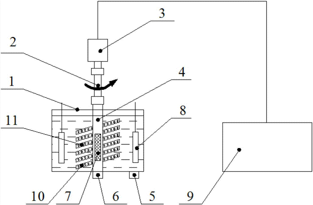
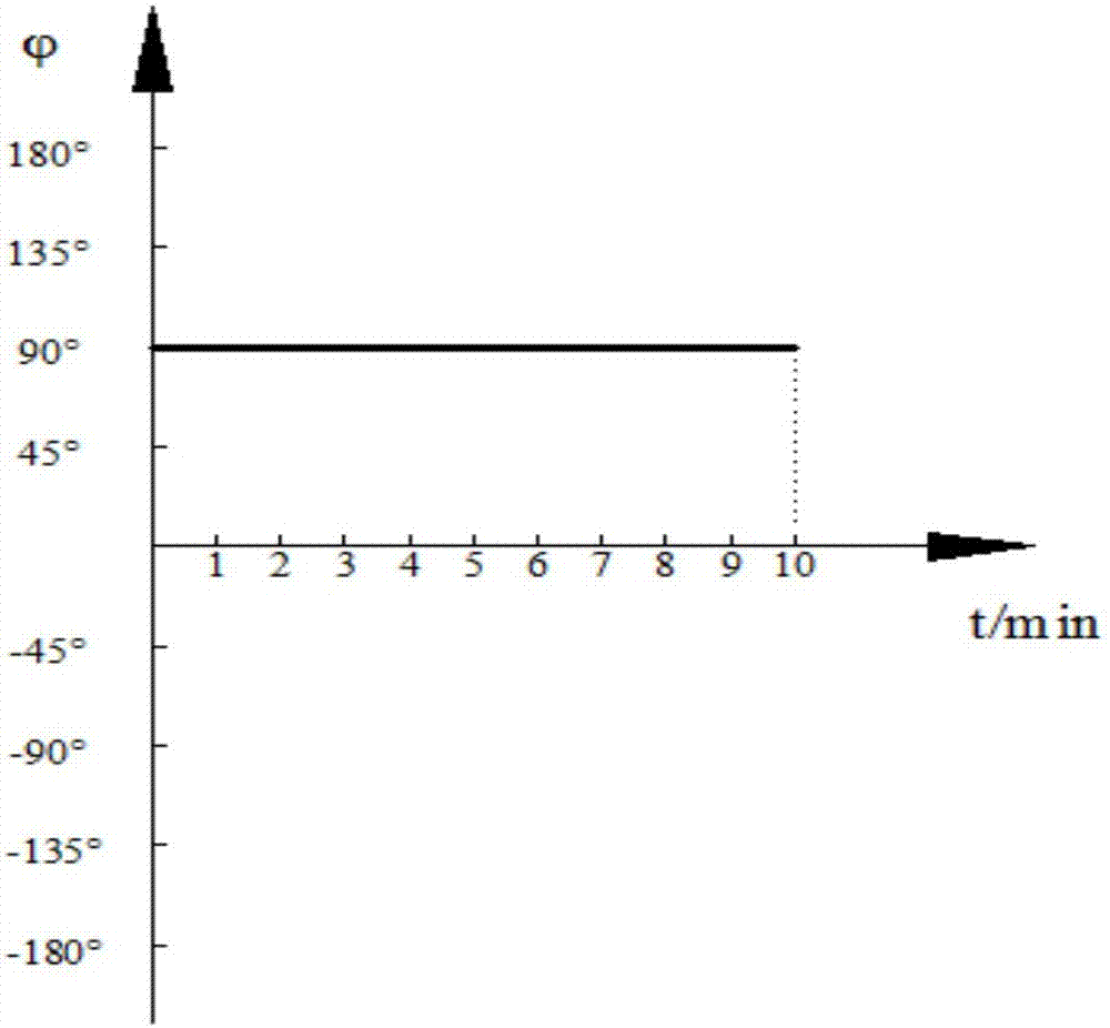
[0047] In this embodiment, the geometric dimension of the blind hole on the circuit board: 100 μm (diameter) × 50 μm (depth); figure 2 shown in The operation procedure of the jet flow device as a parameter is as follows: the jet angle is 90° and lasts for 10 minutes. One cycle is 10min, and the total plating time is 1h.
[0048] Pretreatment conditions: Soak for 5 minutes under the condition of 25L / min jet flow.
[0049] Basic plating solution ratio: 200g / L copper sulfate pentahydrate, 50g / L sulfuric acid, and 99mg / L sodium chloride, and the rest is water.
[0050] Additives include inhibitor, brightener and leveling agent, inhibitor: brightener: leveling agent=100ppm: 10ppm: 5ppm. In this embodiment, the inhibitor is polyethylene glycol, the brightener is sodium polydithiodipropane sulfonate, and the leveling agent is Kenna Green B.
[0051] Experimental conditions: temperature = 25°C, flow rate = 15L / min, current density = 2A / dm 2 , Plating time = 60min.
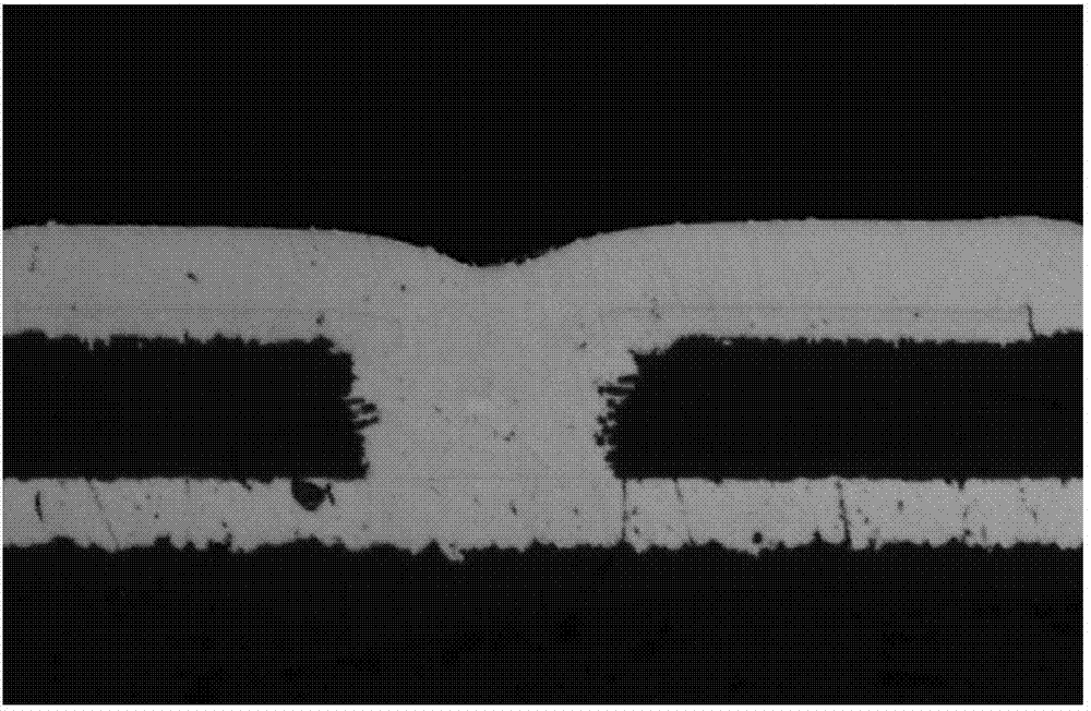
[0052] Res...
Embodiment 2
[0054] In this embodiment, the geometric dimension of the blind hole on the circuit board: 100 μm (diameter) × 50 μm (depth); Figure 4 shown in The operation procedure of the jet flow device as a parameter is as follows: jet angle 45°, last 1min; jet angle 90°, last 2min; jet angle 135°, last 1min; jet angle 180°, last 1min; jet angle -180°, Last 1min; spray angle -135°, last 1min; spray angle -90°, last 2min; spray angle -45°, last 1min. One cycle is 10min, and the total plating time is 1h.
[0055] Pretreatment conditions: Soak for 5 minutes under the condition of 25L / min jet flow.
[0056] Basic plating solution ratio: 200g / L copper sulfate pentahydrate, 50g / L sulfuric acid, and 99mg / L sodium chloride, the rest is water.
[0057] Additives include inhibitor, brightener and leveling agent, inhibitor: brightener: leveling agent=100ppm: 10ppm: 5ppm. In this embodiment, the inhibitor is polyethylene glycol, the brightener is sodium polydithiodipropane sulfonate, and the l...
Embodiment 3
[0061] In this embodiment, the geometric dimension of the blind hole on the circuit board: 150 μm (diameter) × 80 μm (depth); Figure 6 shown in The operation procedure of the jet flow device as a parameter is as follows: spray angle 0°, last 1min; spray angle 90°, last 3min; spray angle 180°, last 1min; spray angle -180°, last 1min; spray angle -90° , lasted 3min; spray angle 0°, lasted 1min. One cycle is 10min, and the total plating time is 1h.
[0062] Pretreatment conditions: Soak for 5 minutes under the condition of 25L / min jet flow.
[0063] Basic plating solution ratio: 200g / L copper sulfate pentahydrate, 50g / L sulfuric acid, and 99mg / L sodium chloride, the rest is water.
[0064] Additives include inhibitor, brightener and leveling agent, inhibitor: brightener: leveling agent=100ppm: 10ppm: 8ppm. In this embodiment, the inhibitor is polypropylene glycol, the brightener is sodium phenyldithiopropane sulfonate, and the leveling agent is thiourea.
[0065] Experimen...
PUM
| Property | Measurement | Unit |
|---|---|---|
| thickness | aaaaa | aaaaa |
| pore size | aaaaa | aaaaa |
| depth | aaaaa | aaaaa |
Abstract
Description
Claims
Application Information
 - R&D
- Intellectual Property
- Life Sciences
- Materials
- Tech Scout
- Unparalleled Data Quality
- Higher Quality Content
- 60% Fewer Hallucinations
Browse by: Latest US Patents, China's latest patents, Technical Efficacy Thesaurus, Application Domain, Technology Topic, Popular Technical Reports.
© 2025 PatSnap. All rights reserved.Legal|Privacy policy|Modern Slavery Act Transparency Statement|Sitemap|About US| Contact US: help@patsnap.com