FA<0.85>Cs<0.15>PbI<3> membrane-based broadband superspeed photodetector and preparation method thereof

A photodetector, ultra-high-speed technology, applied in photovoltaic power generation, electric solid-state devices, semiconductor/solid-state device manufacturing, etc. problem, to achieve uniform size, improve device performance, and strong anti-electromagnetic interference effects

Active Publication Date: 2017-11-03
HEFEI UNIV OF TECH
View PDF4 Cites 24 Cited by
  • Summary
  • Abstract
  • Description
  • Claims
  • Application Information

AI Technical Summary

Problems solved by technology

At present, in the ultraviolet region, most of the photodetectors are made of inorganic materials such as silicon-based or silicon carbide. Due to the harsh manufacturing conditions of these inorganic devices, such as high cost and relatively complicated manufacturing process, they are expensive and heavy. And it is difficult to apply photoelectric conversion with a narrow band range and a wide range
If it is necessary to develop a photodetector device that responds in the spectral range from ultraviolet to visible light, it needs to be realized by preparing a multilayer device, which further increases the manufacturing cost of the device and the complexity of the process.

Method used


Image

  • FA&lt;0.85&gt;Cs&lt;0.15&gt;PbI&lt;3&gt; membrane-based broadband superspeed photodetector and preparation method thereof
  • FA&lt;0.85&gt;Cs&lt;0.15&gt;PbI&lt;3&gt; membrane-based broadband superspeed photodetector and preparation method thereof
  • FA&lt;0.85&gt;Cs&lt;0.15&gt;PbI&lt;3&gt; membrane-based broadband superspeed photodetector and preparation method thereof

Examples


Embodiment 1

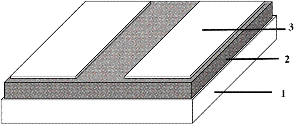
[0027] see figure 1 , the photodetector of the present embodiment is provided with FA on the upper surface of insulating glass 1 0.85 Cs 0.15 PB 3 Film 2, in FA 0.85 Cs 0.15 PB 3 Film 2 is provided with a pair of fa 0.85 Cs 0.15 PB 3The thin film is a gold thin film electrode 3 in ohmic contact.

[0028] Among them: the insulating glass used is ordinary quartz glass with a thickness of 1.2mm; FA 0.85 Cs 0.15 PB 3 The thin film is an n-type perovskite material; the gold thin film electrode is obtained by electron beam evaporation with a thickness of 50nm.

[0029] The photodetector of the present embodiment is prepared according to the following steps:

[0030] (1) Clean the insulating glass with acetone, alcohol and deionized water in sequence, and then dry it with nitrogen; then put it into the vacuum chamber of the plasma cleaning machine, and vacuumize it. -1 Pa, fill in oxygen to adjust the air pressure to 5Pa, press the start button to clean the sample for te...


PUM


Abstract

The invention discloses a FA<0.85>Cs<0.15>PbI<3> membrane-based broadband superspeed photodetector and a preparation method thereof. A FA<0.85>Cs<0.15>PbI<3> membrane is arranged on the upper surface of insulating glass, and a pair of gold membrane electrode in ohmic contact with the membrane is arranged on the FA<0.85>Cs<0.15>PbI<3> membrane. Due to use of the characteristic of a large specific surface area of the FA<0.85>Cs<0.15>PbI<3> membrane and full use of the super high electronic mobility of the membrane, the photodetector has superfast response speed, high light absorption performance, and high electromagnetic immunity, and can sense light ranging from ultraviolet to visible light flexibly. The invention raises new prospect for application of Perovskite materials in the photodetector.

Description

technical field [0001] The invention belongs to the field of semiconductor photodetectors, in particular to a broadband ultra-high-speed photodetector based on iodine-lead-cesium formamidine thin film and a preparation method thereof. Background technique [0002] With the rapid development of modern science and technology, photodetectors (PD) are of great significance in scientific research, production, military affairs, optical research and other fields. Since wide-absorption photodetectors have a wide range of applications in the fields of industry and science and technology, so far many people have combined different functional materials to find a wide-band light-absorbing material, so as to produce a photodetector that can absorb light from ultraviolet photodetectors in the visible region. Different detection devices have different application fields. For example, ultraviolet light region detectors can be used for ultraviolet guidance, detection of cancer cells, observ...

Claims


Application Information

Patent Timeline
Patent Type & Authority Applications(China)
IPC IPC(8): H01L51/42H01L51/46H01L51/48
CPCH10K71/12H10K85/00H10K85/30H10K30/451Y02E10/549
Inventor 梁凤霞王九镇梁林童小伟王迪罗林保
Owner HEFEI UNIV OF TECH
Why Eureka
Try Eureka