A packaging method for mems devices based on lcp multilayer stacking technology

A device packaging, multi-layer stacking technology, applied in radar systems/subsystems, microwave communication fields, can solve the problems of poor air tightness, high loss, low degree of generalization of MEMS devices, etc., to maintain the original performance, low moisture absorption rate , good insulation effect

Active Publication Date: 2019-02-19
NO 54 INST OF CHINA ELECTRONICS SCI & TECH GRP
View PDF6 Cites 34 Cited by
  • Summary
  • Abstract
  • Description
  • Claims
  • Application Information

AI Technical Summary

Problems solved by technology

[0004] The purpose of the present invention is to provide a MEMS device packaging method based on LCP multilayer stacking technology, which is used to solve the technical problems of low generalization, poor airtightness and high loss of MEMS devices

Method used


Image

  • A packaging method for mems devices based on lcp multilayer stacking technology
  • A packaging method for mems devices based on lcp multilayer stacking technology
  • A packaging method for mems devices based on lcp multilayer stacking technology

Examples


Embodiment Construction

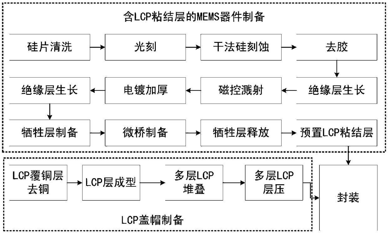
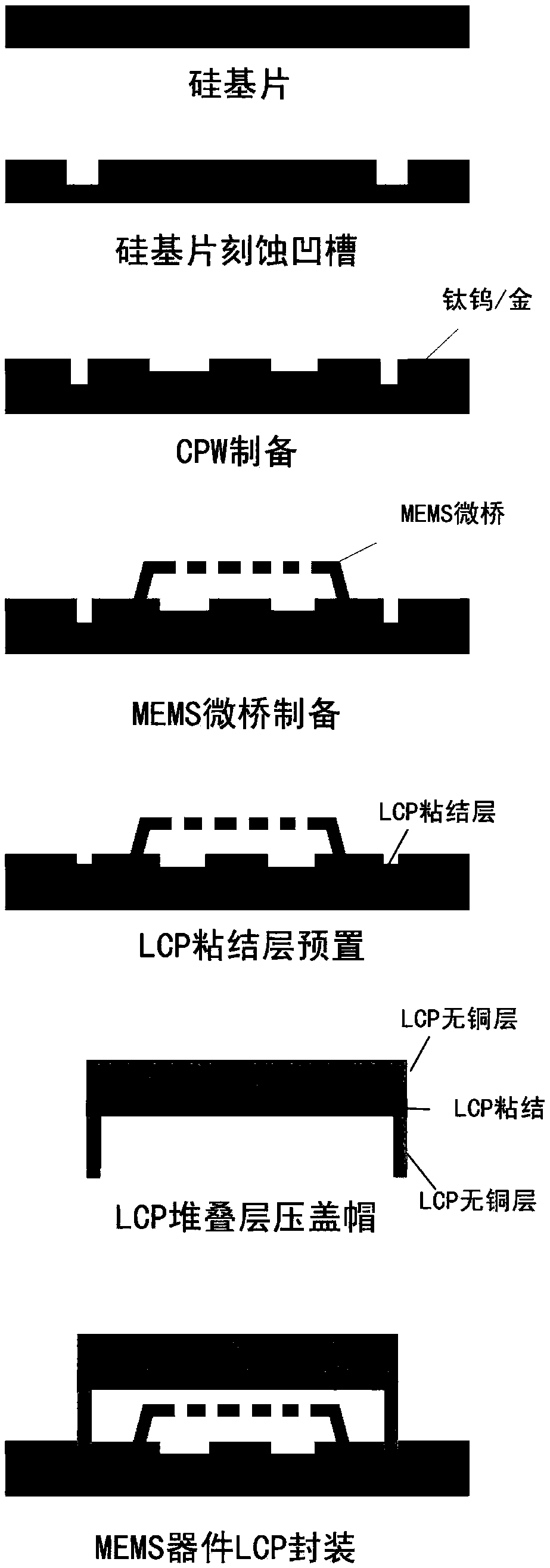
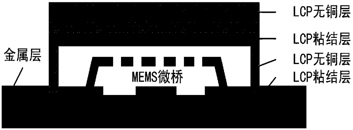
[0039] Below, combine figure 1 , figure 2 and image 3 The present invention is further described.

[0040] A MEMS device packaging method based on LCP multilayer stacking technology, its processing process is as follows figure 1 As shown, it specifically includes the following steps:

[0041] (1) Cleaning the silicon substrate with an organic cleaning solution.

[0042] Place a silicon substrate with a diameter of 100 mm, a thickness of 0.4 mm, and double-sided polishing in a beaker filled with acetone, use ultrasonic cleaning for 5 to 10 minutes, and then take out the silicon substrate and place it in a beaker filled with alcohol. Use ultrasonic cleaning for 5 minutes to 10 minutes to clean the dirt on the surface of the silicon substrate, and take it out for later use after cleaning.

[0043] (2) photolithography is carried out to the front side of the silicon substrate after cleaning in step (1), and a mask pattern of dry etching silicon grooves is formed on the fron...


PUM


Abstract

The invention discloses a MEMS device packaging method based on LCP multilayer stacking technology, which is characterized in that the MEMS device is obtained by sputtering, photolithography, etching, electroplating and other processes on a double-sided polished silicon substrate, and at the same time Form silicon grooves that are easy to lead out and have accurate alignment; based on the LCP multilayer stacking technology, on the multilayer LCP substrate, the cap part of the device package is obtained through laser scribing, alignment, lamination and other processes; the device and the cap Package without assistance, high-precision integration, and obtain MEMS devices with low loss and good airtightness. The MEMS device of the invention has the advantages of low loss, high isolation and good airtightness. This method can better provide packaging protection for MEMS devices with movable parts, and is especially suitable for miniaturization applications of microwave, millimeter wave communication, radar and other systems / subsystems, and belongs to the realization of miniaturization, high performance microwave communication, radar systems / The key technology of the subsystem.

Description

technical field [0001] The invention belongs to the key technical field of realizing miniaturized, high-performance, and highly generalized microwave communication and radar systems / subsystems, and specifically relates to a packaging method suitable for MEMS devices based on LCP multilayer stacking technology. Background technique [0002] With the increasing demand for miniaturization of T / R components and microwave / millimeter wave modules in communication systems and phased array radar systems, electronic equipment is gradually developing in the direction of miniaturization and high performance. The integration and performance of modules and components Increase accordingly. MEMS devices have played an increasingly important role in it, becoming a key component in the system to achieve reconfigurability, and its performance and volume directly affect the performance and integration of communication and radar systems / subsystems. [0003] MEMS devices contain moving parts, a...

Claims


Application Information

Patent Timeline
Patent Type & Authority Patents(China)
IPC IPC(8): B81B7/00B81B7/02
CPCB81B7/0032B81B7/02
Inventor 赵飞党元兰徐亚新梁广华刘晓兰唐小平王康
Owner NO 54 INST OF CHINA ELECTRONICS SCI & TECH GRP
Why Eureka
Try Eureka