

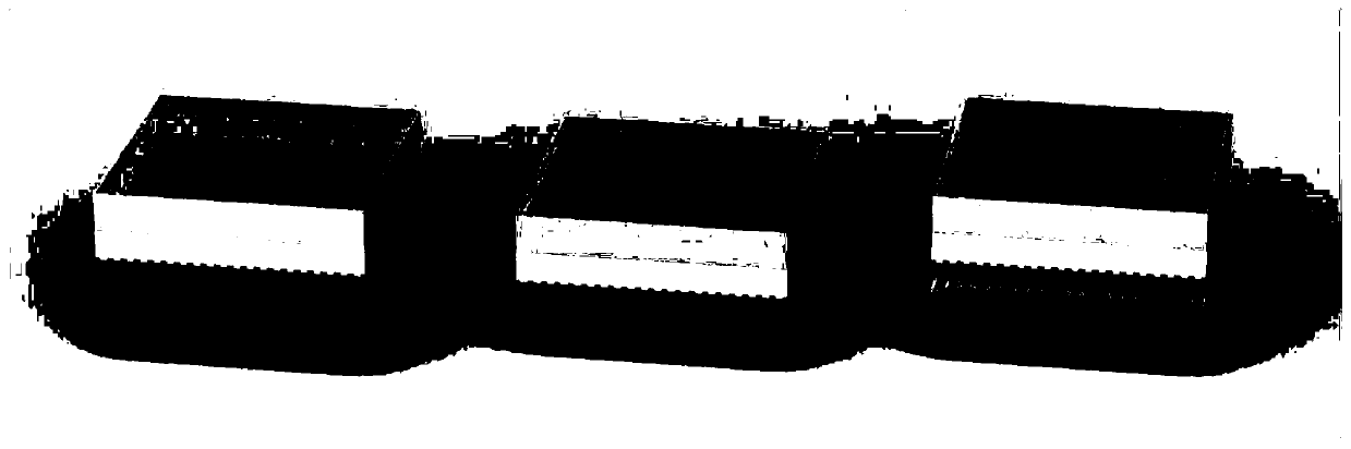
All-Silicon Distributed Feedback Laser
A distributed feedback, laser technology, applied in the laser field, can solve the problems of incompatibility, complex production process, high production cost, etc., and achieve the effect of avoiding incompatibility, compact structure and low cost
- Summary
- Abstract
- Description
- Claims
- Application Information
AI Technical Summary
Problems solved by technology
Method used
Image


Examples
Embodiment Construction
[0045] The following examples are used to illustrate the present invention, but not to limit the present invention.
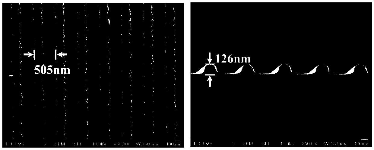
[0046] 1. Raw material and formula:
[0047] Substrate: polished on both sides, volume is 20×20×0.2mm 3 High temperature resistant quartz substrate;
[0048] Template self-assembly anti-sticking layer: 1H, 1H, 2H, 2H-Perfluorooctyltrichlorosilane, Microresist technology company;
[0049] Template adhesion layer: OrmoPrime, Micro resist technology company;
[0050] Template raster layer: OrmoStamp, Micro resist technology company;
[0051] Buff materials: Dow Corning FOx-1x and FOx-2x Flowable Oxides, Dow Corning Corporation;
[0052] Substrate cleaning solution: alcohol (analytical grade), acetone (analytical grade), Sinopharm Chemical Reagent Co., Ltd.;
[0053] 2. Process parameter setting:
[0054] Preparation conditions: room temperature, clean environment;
[0055] Annealing temperature: 1100°C;
[0056] Annealing time: 60 minutes;
[0057] Subseq...
PUM
 Abstract
Description
Claims
Application Information