Semiconductor device and preparation method thereof, and electronic device

A semiconductor and device technology, applied in the field of semiconductor devices and their preparation methods, and electronic devices, can solve problems such as material layer over-etching, device failure, etc., and achieve the effects of improving device performance, reducing area, and reducing the influence of capillary action

Active Publication Date: 2017-11-21
SEMICON MFG INT (SHANGHAI) CORP +1
View PDF5 Cites 0 Cited by
  • Summary
  • Abstract
  • Description
  • Claims
  • Application Information

AI Technical Summary

Problems solved by technology

[0004] In the field of MEMS, there are some products that need to form a cavity in the MEMS device in order to realize the function of the MEMS device. However, during the process of forming the cavity, the material layer above the sacrificial layer may have a special shape, such as a long strip shape. Will cause overetching of the layer of material beneath the part, causing the device to fail

Method used


Image

  • Semiconductor device and preparation method thereof, and electronic device
  • Semiconductor device and preparation method thereof, and electronic device
  • Semiconductor device and preparation method thereof, and electronic device

Examples


preparation example Construction

[0049] In order to solve the above problems, the inventor has carried out in-depth analysis and practice on the causes of the problems, and combined his own experience to propose a method for preparing a semiconductor device, the method comprising:

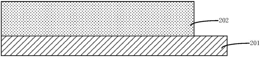
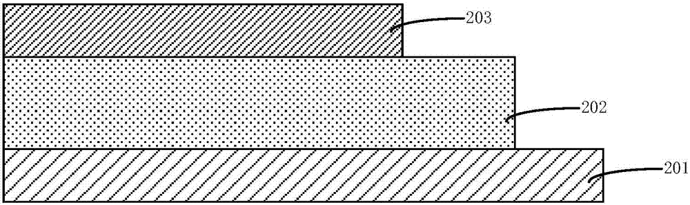
[0050] A semiconductor substrate is provided, on which a first semiconductor material layer, a patterned sacrificial layer and a patterned second semiconductor material layer are sequentially formed, wherein the second semiconductor material layer includes a main chip area and A strip-shaped area located on one side of the main chip area, wherein a strip-shaped etchant barrier layer is formed on both sides of one end of the strip-shaped area close to the main chip area;

[0051] forming spacers on sidewalls of the second semiconductor material layer;

[0052] forming a covering layer on the second semiconductor material layer and the spacer to cover the second semiconductor material layer and the spacer;

[0053] The spacer and t...

Embodiment 1

[0062] Refer below figure 1 with Figure 2a-2e The preparation method of the semiconductor device of the present invention is described in detail, figure 1 Shows a flow chart of the fabrication process of the semiconductor device of the present invention; Figure 2a-2e A schematic cross-sectional view of a structure obtained by sequentially implementing the manufacturing method of the semiconductor device of the present invention is shown.

[0063] The invention provides a method for preparing a semiconductor device, such as figure 1 As shown, the main steps of the preparation method include:

[0064] Step S1: providing a semiconductor substrate on which a first semiconductor material layer, a patterned sacrificial layer and a patterned second semiconductor material layer are sequentially formed, wherein the second semiconductor material layer includes a main A chip area and a strip-shaped area located on one side of the main chip area, wherein a strip-shaped etchant barri...

Embodiment 2

[0119] The present invention also provides a semiconductor device, the semiconductor device comprising:

[0120] semiconductor substrate;

[0121] The first semiconductor material layer 201 is located on the semiconductor substrate;

[0122] The second semiconductor material layer 203 is located above the first semiconductor material layer;

[0123] a cavity located between the first layer of semiconductor material and the second layer of semiconductor material;

[0124] a cover layer 205, located above the second semiconductor material layer and enclosing the cavity;

[0125] Wherein, the second semiconductor material layer includes a main chip area 2031 and a strip-shaped area 2032 located on one side of the main chip area, wherein two sides of one end of the strip-shaped area close to the main chip area are formed with Strip-shaped etchant blocking layer 2034 .

[0126] Wherein the semiconductor substrate (not shown in the figure) may be at least one of the materials ment...


PUM

PropertyMeasurementUnit
thicknessaaaaaaaaaa

Abstract

The invention provides a semiconductor device and a preparation method thereof, and an electronic device. The method comprises the steps of providing a semiconductor substrate, and sequentially forming a first semiconductor material layer, a patterned sacrificial layer and a second patterned semiconductor material layer on the semiconductor substrate, wherein the second semiconductor material layer comprises a master chip area and a strip-shaped area positioned on one side of the master chip area, strip-shaped etching liquid barrier layers are formed on two sides of one end, close to the master chip area, in the strip-shaped area; forming a gap wall on the side wall of the second semiconductor material layer; forming coverage layers on the second semiconductor material layer and the gap wall to cover the same; and removing the gap wall and the sacrificial layer under the master chip area by using a wet etching method so as to form a cavity between the first semiconductor material layer and the second semiconductor material layer. According to the method provided by the invention, the problem that the strip-shaped area is suspending can be solved.

Description

technical field [0001] The invention relates to the technical field of semiconductors, in particular to a semiconductor device, a preparation method, and an electronic device. Background technique [0002] With the continuous development of semiconductor technology, in the market of sensor (motion sensor) products, smart phones, integrated CMOS and micro-electromechanical system (MEMS) devices have increasingly become the most mainstream and advanced technology, and with the update of technology, The development direction of this kind of transmission sensor products is smaller size, high-quality electrical performance and lower loss. [0003] Among them, MEMS sensors are widely used in automotive electronics: such as TPMS, engine oil pressure sensor, air pressure sensor of automobile brake system, automobile engine intake manifold pressure sensor (TMAP), common rail pressure sensor of diesel engine; consumer electronics: such as tire pressure gauge , sphygmomanometer, cabin...

Claims


Application Information

Patent Timeline
Patent Type & Authority Applications(China)
IPC IPC(8): B81C1/00B81B1/00H04R19/04
Inventor 王贤超
Owner SEMICON MFG INT (SHANGHAI) CORP
Why Eureka
Try Eureka