

Graphene buried heat radiation layer and vertical channel GaN MISFET cellular structure and preparation method
A heat-dissipating layer, graphene technology, applied in the direction of electrical components, semiconductor/solid-state device manufacturing, electrical solid-state devices, etc., can solve the problems of high switching rate, low device on-resistance, etc. Polar on-resistance, the effect of reducing the length
- Summary
- Abstract
- Description
- Claims
- Application Information
AI Technical Summary
Problems solved by technology
Method used
Image

Examples
Embodiment Construction
[0032] The present invention will now be described more fully with reference to the accompanying drawings, in which exemplary embodiments of the invention are shown. This invention may, however, be embodied in many different forms and should not be construed as limited to the exemplary embodiments set forth herein. Rather, these embodiments are provided so that this disclosure will be thorough and complete, and will fully convey the scope of the invention to those skilled in the art.
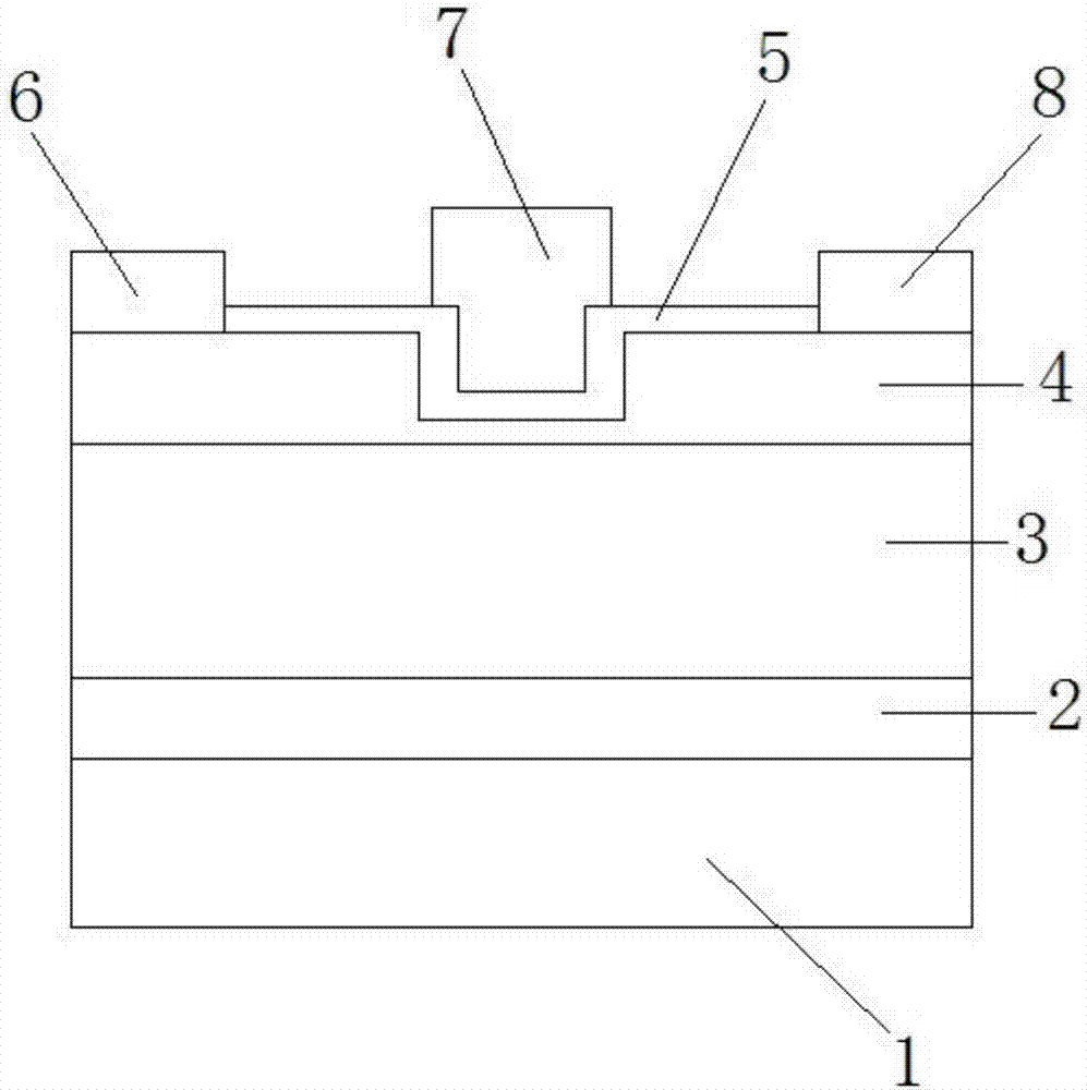
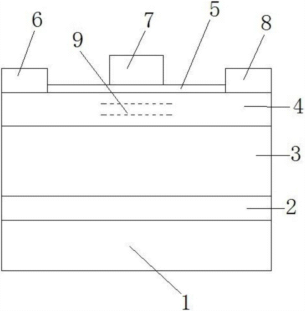
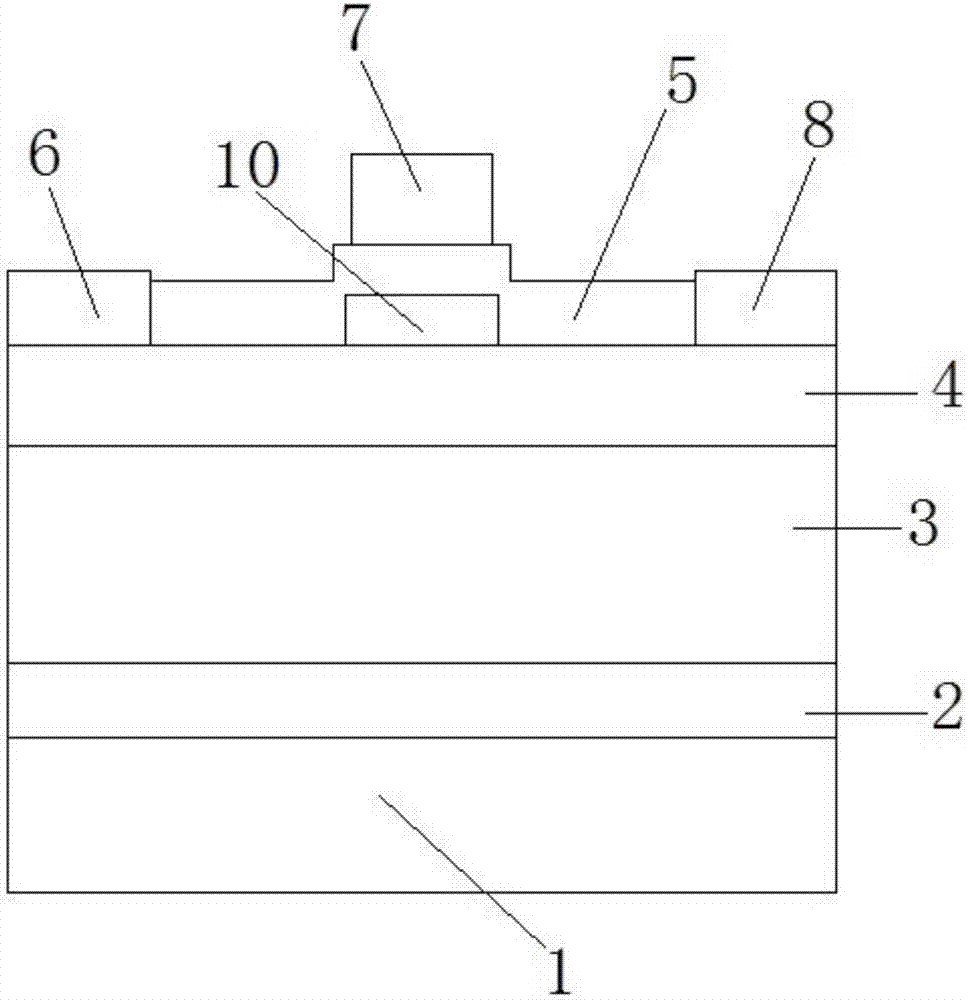
[0033] like Figure 4-5As shown, the present invention provides a graphene buried heat dissipation layer and a vertical channel GaN MISFET cellular structure, which comprises a substrate 11, an AlN isolation layer 12, a graphene buried heat dissipation layer 13, an AlN formed Nucleus layer 14, GaN buffer layer 15, n-type heavily doped GaN layer 16, n-type GaN layer 17, p-type GaN electron blocking layer 18, undoped GaN layer 19 and AlGaN barrier layer 20; the gate of the cellular structure The...
PUM
| Property | Measurement | Unit |
|---|---|---|
| Thickness | aaaaa | aaaaa |
| Thickness | aaaaa | aaaaa |
Abstract
Description
Claims
Application Information