Oxide thin film transistor device based on composite insulation layer and preparation method of oxide thin film transistor device

A technology of oxide film and composite insulation, which is applied in the field of electronics, can solve the problems of high roughness IGZO thin film transistors, high cost of alumina surface, long preparation time, etc., and achieve the goal of reducing roughness, good compactness, and reducing surface defects Effect

Active Publication Date: 2017-11-28
UNIV OF ELECTRONICS SCI & TECH OF CHINA
View PDF3 Cites 7 Cited by
  • Summary
  • Abstract
  • Description
  • Claims
  • Application Information

AI Technical Summary

Problems solved by technology

[0004] The object of the present invention is to solve the problem of the high roughness of reactive sputtering alumina surface and the damage of pinhole phenomenon to the performance of IGZO thin-film transistors or the method of molecular beam epitaxy to prepare alumina surface has relatively high cost and long preparation time, and To solve the problem of exhaust gas, the invention provides an oxide thin film transistor device based on a composite insulating layer and its preparation method

Method used


Image

  • Oxide thin film transistor device based on composite insulation layer and preparation method of oxide thin film transistor device
  • Oxide thin film transistor device based on composite insulation layer and preparation method of oxide thin film transistor device
  • Oxide thin film transistor device based on composite insulation layer and preparation method of oxide thin film transistor device

Examples


example 1

[0037] like Figure 4 As shown, an oxide thin film transistor device based on a composite insulating layer includes 1-substrate, 2-gate electrode, 3-composite insulating layer, 4-oxide semiconductor layer, 5-source electrode, 6-drain electrode .

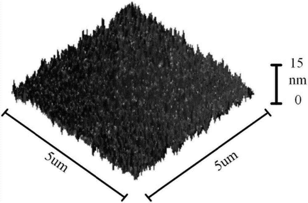
[0038] Specific structure: the substrate is ITO glass substrate, the gate electrode is ITO (200nm), and the composite insulating layer is Al 2 o 3 The insulating layer (110 nm), the oxide semiconductor layer is IGZO (50 nm), and the source electrode and drain electrode are Ag (60 nm).

[0039] A method for preparing an oxide thin film transistor device based on a single-layer insulating layer, comprising the following steps:

[0040] S1: Clean the glass substrate 1: (a) Gently wipe the ITO glass substrate with a dust-free cloth stained with acetone to remove large particles of impurities on the glass substrate; (b) put the cleaned glass on the Put the substrate frame into a glass beaker filled with acetone on the polytetrafluoroe...

example 2

[0047] like Figure 4 As shown, an oxide thin film transistor device based on a composite insulating layer includes 1-substrate, 2-gate electrode, 3-composite insulating layer, 31-alumina, 32-organic, 4-oxide semiconductor layer, 5-source electrode, 6-drain electrode.

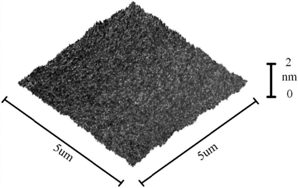
[0048] Specific structure: substrate is ITO glass substrate, gate electrode is ITO (200nm), composite insulating layer Al 2 o 3 The insulating layer (110nm) / PMMA (50nm), the oxide semiconductor layer is IGZO (50nm), and the source electrode and drain electrode are Ag (60nm).

[0049] An oxide thin film transistor device based on a composite insulating layer and a preparation method thereof, comprising the following steps:

[0050] S1: Clean the glass substrate 1: (a) Gently wipe the ITO glass substrate with a dust-free cloth stained with acetone to remove large particles of impurities on the glass substrate; (b) put the cleaned glass on the Put the substrate frame into a glass beaker filled with acetone on ...

example 3

[0057] like Figure 4 As shown, an oxide thin film transistor device based on a composite insulating layer includes 1-substrate, 2-gate electrode, 3-composite insulating layer, 31-alumina, 32-organic, 4-oxide semiconductor layer , 5-source electrode, 6-drain electrode.

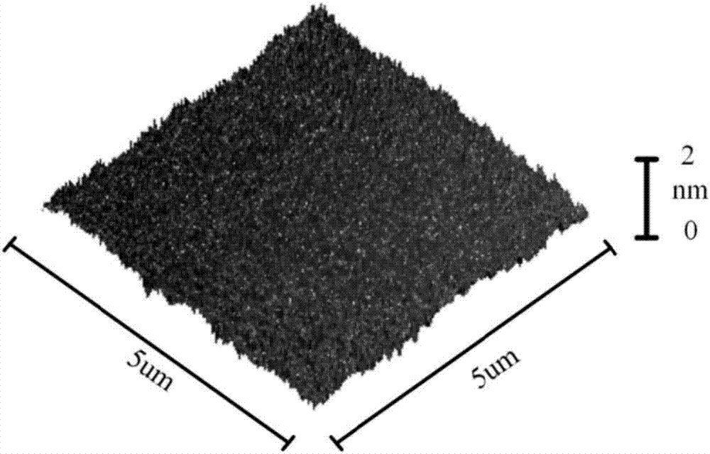
[0058] Specific structure: substrate is ITO glass substrate, gate electrode is ITO (200nm), composite insulating layer Al 2 o 3 The insulating layer (110nm) / PVA (40nm), the oxide semiconductor layer is IGZO (50nm), and the source electrode and drain electrode are Ag (60nm).

[0059] An oxide thin film transistor device based on a composite insulating layer and a preparation method thereof, comprising the following steps:

[0060] S1: Clean the glass substrate 1: (a) Gently wipe the ITO glass substrate with a dust-free cloth stained with acetone to remove large particles of impurities on the glass substrate; (b) put the cleaned glass on the Put the substrate frame into a glass beaker filled with acetone on ...


PUM

PropertyMeasurementUnit
thicknessaaaaaaaaaa
thicknessaaaaaaaaaa
thicknessaaaaaaaaaa

Abstract

The invention discloses an oxide thin film transistor device based on composite insulation layer and a preparation method of the oxide thin film transistor device, and belongs to the technical field of electronics. The objective of the invention is to solve the problem of damage to performance of an IGZO thin film transistor caused by phenomenon of high roughness and appearance of a pin hole of the reactive sputtering aluminum oxide surface. According to the invention, the device comprises a substrate, a gate electrode, the composite insulation layer, an oxide semiconductor layer, a source electrode and a drain electrode, which are successively arranged up and down, wherein the source electrode and the drain electrode are arranged on the oxide semiconductor layer, the composite insulation layer comprises upper and lower layers, the lower layer is the aluminum oxide on the gate electrode and the upper layer is the organic material on the aluminum oxide. Thus, performance of the thin film transistor is improved.

Description

technical field [0001] An oxide thin film transistor device based on a composite insulating layer and a preparation method thereof are used for thin film transistors and belong to the field of electronic technology. Background technique [0002] In recent years, metal-oxide thin-film transistors (TFTs) have attracted extensive attention for their potential applications in the field of active-matrix light-emitting diode (AM-OLED) displays. Traditional amorphous silicon TFTs cannot meet the requirements of AM-OLED display current-mode drive mode due to low carrier mobility and severe threshold voltage drift; although polysilicon TFTs have high carrier mobility and stable However, limited by the size of laser crystallization and other processes, the existence of a large number of grain boundaries in the film makes the uniformity of mobility poor when preparing large-scale devices, which affects the application in the field of AM-OLED display. Metal oxide TFTs not only have hig...

Claims


Application Information

Patent Timeline
Patent Type & Authority Applications(China)
IPC IPC(8): H01L29/786H01L21/336
CPCH01L29/66742H01L29/78603
Inventor 张磊周斌张珊珊袁毅刘腾飞
Owner UNIV OF ELECTRONICS SCI & TECH OF CHINA
Why Eureka
Try Eureka