Preparation method of stretchable crystalline semiconductor nanowire based on linear design and guidance of planar nanowire

A nanowire and semiconductor technology, which is applied in the production field of spring structure crystal nanowires, can solve the problems that the existing technology is not very good, and achieve the effects of facilitating integration and use, and improving device characteristics and stability.

Inactive Publication Date: 2017-12-12
NANJING UNIV
View PDF0 Cites 25 Cited by
  • Summary
  • Abstract
  • Description
  • Claims
  • Application Information

AI Technical Summary

Problems solved by technology

[0005] The growth of materials with stretchable crystalline nanowire spring structure is the basis of flexible and stretchable electronic devices, and the existing technology does not have a good way to solve it

Method used


Image

  • Preparation method of stretchable crystalline semiconductor nanowire based on linear design and guidance of planar nanowire
  • Preparation method of stretchable crystalline semiconductor nanowire based on linear design and guidance of planar nanowire
  • Preparation method of stretchable crystalline semiconductor nanowire based on linear design and guidance of planar nanowire

Examples


Embodiment Construction

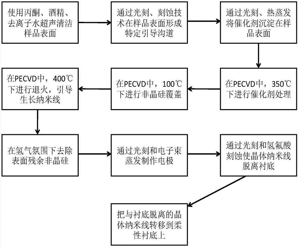
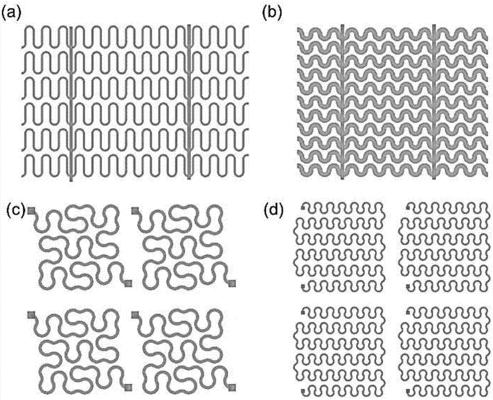
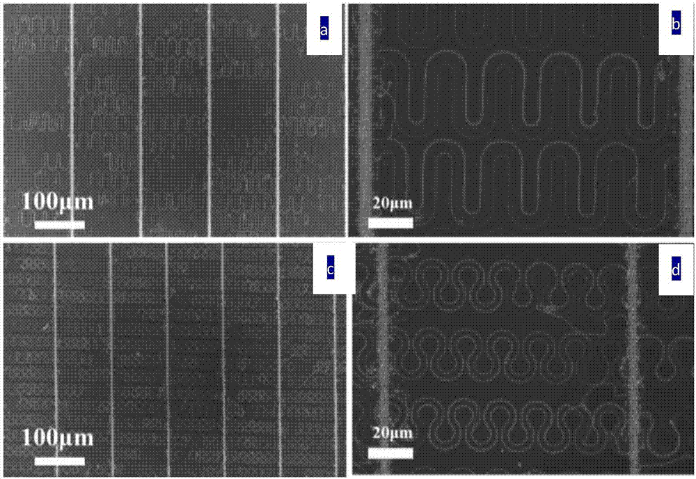
[0030] In order to make the objectives, technical solutions, functions and advantages of the present invention more clear, the following will further explain the present invention in detail with reference to specific examples. Flow chart attached figure 1 Shown. A linear design and guided growth technology based on planar nanowires realizes a preparation method of crystalline semiconductor (including silicon, germanium, etc.) stretchable electronic devices. Using conventional photolithography, etching techniques, or other template and surface processing techniques, a guide step with a specific shape is made on a glass or crystalline silicon substrate, and an amorphous thin film (using amorphous silicon, amorphous germanium and other amorphous silicon Crystalline inorganic semiconductor materials) are used as precursors, using metal (indium, tin, gallium, bismuth, etc.) catalytic particles to absorb amorphous films, and in the process of guiding the movement of the steps, the co...


PUM

PropertyMeasurementUnit
thicknessaaaaaaaaaa
diameteraaaaaaaaaa
diameteraaaaaaaaaa

Abstract

A preparation method of a stretchable crystalline semiconductor nanowire based on linear design and guidance of a planar nanowire comprises the steps that 1, standardized cleaning is conducted on glass, silicon dioxide sheet or a silicon wafer substrate; 2, a photoetching or surface pattern etching technology is utilized to etch a step having a certain depth on the surface of the substrate; 3, the crystal nanowire with the diameter of about 130 +/- 20 nm accurately grows along a guiding channel through a planar nanowire guidance growth method to form a nanowire spring array; 4, a metal film is treatment in a PECVD system by utilizing reductive plasmas including hydrogen and the like to form nano metal catalysis particles in the range from dozens of nanometers to one micrometer; 5, an amorphous semiconductor layer having appropriate thickness deposits in a covering mode to serve as a precursor medium; 6, annealing growth is performed in a vacuum or nonoxidative atmosphere, and an amorphous layer is absorbed and a crystalline nanowire structure deposits in the way at the temperature of 250 DEG C or above.

Description

1. Technical Field [0001] The invention relates to the field of flexible and stretchable electronics and devices, and relates to a method for using a channel to guide the growth of planar nanowires on a substrate, and through a micromachining process, to produce a spring structure crystalline nanowire with flexible and stretchable properties . In particular, it is a method for channel-guided self-positioning self-directed growth, transfer, and electrical integration of planar semiconductor nanowires to prepare spring structure crystalline nanowires. 2. Technical background [0002] With the development of the contemporary electronic display industry, flexible and stretchable electronic devices (especially display devices) are more likely to meet actual application requirements and their own flexible material characteristics. They are playing more and more important roles in modern technology, national economy and daily life. An increasingly important role, in this research field...

Claims


Application Information

Patent Timeline
Patent Type & Authority Applications(China)
IPC IPC(8): C30B25/18C30B29/60C30B29/06C30B29/08
CPCC30B25/183C30B25/186C30B29/06C30B29/08C30B29/406C30B29/60B82Y10/00B82Y40/00H01L21/02381H01L21/02422H01L21/0243H01L21/02532H01L21/02546H01L21/02587H01L21/02592H01L21/02603H01L21/02639H01L21/02645H01L21/02653H01L29/0673H01L29/775C30B29/42H01L21/02598H01L21/02658H01L29/0669
Inventor 余林蔚薛兆国董泰阁王军转
Owner NANJING UNIV
Why Eureka
Try Eureka