Super flexible nitride-based pyramid structure semiconductor device and preparation method thereof

A base pyramid, gallium nitride technology, applied in semiconductor devices, electrical components, circuits, etc., can solve the problems of device size limitation, micro-nano structure damage, difficult to achieve high flexibility devices, etc., to improve efficiency and size. Restricted, guaranteed size effect

Inactive Publication Date: 2017-12-15
XI AN JIAOTONG UNIV
View PDF3 Cites 15 Cited by
  • Summary
  • Abstract
  • Description
  • Claims
  • Application Information

AI Technical Summary

Problems solved by technology

The separation process of the device is generally through chemical corrosion or mechanical peeling, which will inevitably cause irreversible damage to the micro-nano structure.
Even if the above problems are not considered, previous reports are difficult to achieve highly flexible devices, and the size of the devices is also limited, mainly because they still have problems in the electrode fabrication process of the devices.

Method used


Image

  • Super flexible nitride-based pyramid structure semiconductor device and preparation method thereof
  • Super flexible nitride-based pyramid structure semiconductor device and preparation method thereof
  • Super flexible nitride-based pyramid structure semiconductor device and preparation method thereof

Examples


preparation example Construction

[0040] The preparation method of ultra-flexible GaN-based pyramid structure semiconductor device of the present invention comprises the following steps:

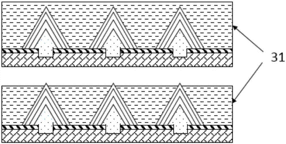
[0041] 1) SiO 2 The mask 12 is covered on the sapphire substrate 11, and then on the SiO 2 Patterning is carried out on the mask 12 and the sapphire substrate 11 to obtain a patterned substrate, then a pyramid array 2 is grown on the patterned substrate, and the gap between each pyramid in the pyramid array 2 is filled by an insulating filling material 31 , and etch to expose the top of each pyramid in the pyramid array 2;

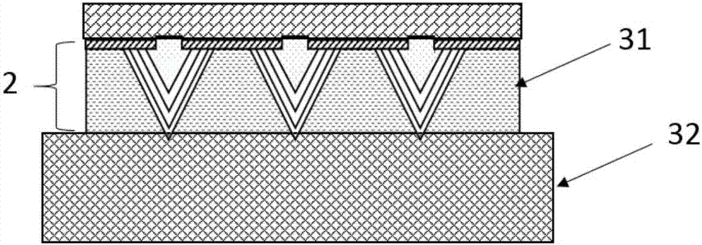
[0042] 2) transfer the pyramid array 2 to the semi-cured PDMS temporary substrate 32, wherein, the top of each pyramid in the pyramid array 2 faces down and is connected with the semi-cured PDMS temporary substrate 32, then peels off the sapphire substrate 11, Then the pyramid array 2, the semi-cured PDMS temporary substrate 32 and SiO 2 The structure that mask 12 forms rotates in vertical direction, ...

Embodiment 1

[0049] The making process of the present invention is:

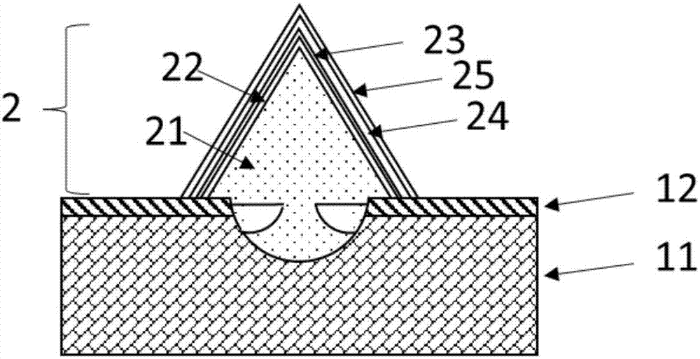
[0050] 1) Reference figure 1 , covered with SiO 2 On the sapphire substrate 11 of mask 12, carry out patterning by the mode of laser drilling, obtain patterned substrate, then grow pyramid array 2 on the substrate of described patterning, the structure of each pyramid in pyramid array 2 can be Design according to the requirements of different devices, taking light-emitting diode devices as an example, each pyramid in the pyramid array 2 includes 2um thick unintentionally doped gallium nitride 21, 1um thick n-type gallium nitride layer 22, 10 groups of quantum wells and 100nm thick p-type gallium nitride layer 24;

[0051] 2) The p-type gallium nitride layer 24 has a very high resistivity. In order to ensure the uniformity of the current distribution on the pyramid, a transparent conductive layer 25 of 100nm-200nm is deposited on the surface of the pyramid. The material of the transparent conductive layer 25 is ITO or ...


PUM

PropertyMeasurementUnit
widthaaaaaaaaaa
lengthaaaaaaaaaa

Abstract

The invention discloses a super flexible nitride-based pyramid structure semiconductor device and a preparation method thereof; the semiconductor device comprises a flexible substrate, a conductive bonding layer, a SiO2 mask layer, a pyramid array and a P-surface transparent electrode arranged in order from bottom to top; an insulation filler is filled between pyramids in the pyramid array; each pyramid in the array comprises a pyramid structure unintentional doping gallium nitride, and a n-type gallium nitride layer, a quantum well layer, a p-type gallium nitride layer and a transparent conductive layer covering the unintentional doping gallium nitride in order; the bottom of the unintentional doping gallium nitride penetrates the SiO2 mask layer and is connected with the conductive bonding layer; the top of the transparent conductive layer is connected with the P-surface transparent electrode; the semiconductor device is not limited in size, high in flexibility, and the preparation method is simple, convenient and easy to realize.

Description

technical field [0001] The invention belongs to the technical field of semiconductors, and relates to an ultra-flexible gallium nitride-based pyramid structure semiconductor device and a preparation method thereof. Background technique [0002] In recent years, the wide application of flexible electronics and optics in wearable smart electronics, light-emitting devices, solar cells, sensors and biology has attracted the attention of many researchers. Gallium nitride-based semiconductor devices have become one of the most important choices to replace organic semiconductor devices due to their excellent material properties, thermal and electrical stability, higher quantum efficiency and luminous efficiency. However, since the gallium nitride material itself is a hard material and has poor flexibility, in order to avoid device failure due to cracks caused by bending during the process and practical application, the entire gallium nitride film needs to be cut into micron-sized d...

Claims


Application Information

Patent Timeline
Patent Type & Authority Applications(China)
IPC IPC(8): H01L33/00H01L33/06H01L33/32H01L33/40
CPCH01L33/0066H01L33/0075H01L33/0093H01L33/06H01L33/32H01L33/40
Inventor 云峰李虞锋田振寰
Owner XI AN JIAOTONG UNIV
Why Eureka
Try Eureka