Thick copper sandwiched aluminum substrate manufacturing method

A sandwich aluminum substrate and a manufacturing method are used in printed circuit manufacturing, metal core circuit manufacturing, electrical components, etc., and can solve problems such as short circuits and scrap aluminum substrates, so as to avoid short circuits, reduce product defect rates, and achieve good economic benefits. Effect

Active Publication Date: 2017-12-15
深圳明阳电路科技股份有限公司
View PDF10 Cites 11 Cited by
  • Summary
  • Abstract
  • Description
  • Claims
  • Application Information

AI Technical Summary

Problems solved by technology

In the traditional aluminum substrate manufacturing process, when making through holes, it is usually directly drilled from thick copper into the aluminum su

Method used


Image

  • Thick copper sandwiched aluminum substrate manufacturing method
  • Thick copper sandwiched aluminum substrate manufacturing method

Examples


Embodiment 1

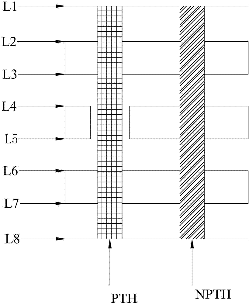
[0021] Such as figure 2 As shown, it shows a thick copper sandwich aluminum substrate, the structure is: L2-3 layer (upper sub-board) and L6-7 layer (lower sub-board) are FR4 sheet material, Tg180, thickness 0.25±0.038mm (no Contains copper), copper thickness H / Hoz; L4-5 layer (aluminum substrate) is a double-sided aluminum-based core board, aluminum base 1.00mm, insulating dielectric layer thickness 0.08-0.10mm, copper thickness 5 / 5oz; between layers The bonding sheet medium is FR4 prepreg.

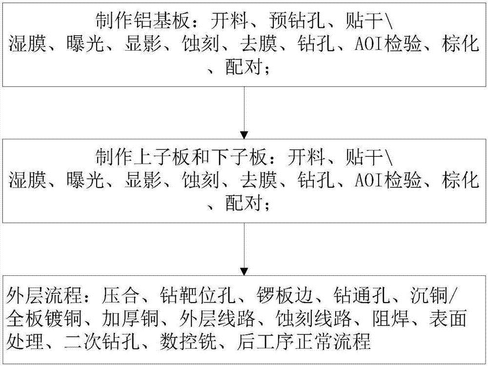
[0022] According to the characteristics of the sheet material and related process requirements and the production experience of the original printed circuit board, we have formulated a production process for the test board: daughter board L4-5 layer process: cutting material → etching isolation ring film → etching isolation ring → Drill target holes → Pre-drill holes → Resin plug holes → Grinding plate → Copper covering production → L4-5 layer circuit production → Line etching → Inspec...


PUM


Abstract

The invention discloses a thick copper sandwiched aluminum substrate manufacturing method, which comprises the following steps: (1) making an aluminum substrate: opening a material, pre-drilling, dry or wet film sticking, exposing, developing, etching, hole drilling, AOI testing, browning, and pairing; (2) making an upper board and a lower board: opening the material, dry or wet film sticking, exposing, developing, etching, film removing, hole drilling, AOI testing, browning, and pairing; (3) and performing outer layer processing: pressing and fitting, drilling a target position hole, gonging plate edge, drilling a through hole, copper sinking/full plate copper plating, thickening copper, outer line wiring, etching lines, soldering, surface treating, secondary drilling, CNC milling, and process-post normal processes. The method pre-drills a hole on an aluminum substrate to prevent the short circuit between the copper clad layer and the aluminum base during drilling, thereby reducing the product defect rate and possessing good economic benefits.

Description

technical field [0001] The invention relates to the technical field of a method for manufacturing a metal core board of a circuit board, in particular to a method for manufacturing a thick copper sandwich aluminum substrate. Background technique [0002] With the development of light, thin, small, high-density and multi-functional electronic products, the assembly density and integration of components on printed boards are getting higher and higher, the power consumption is getting bigger and bigger, and the heat dissipation requirements of PCB substrates are getting higher and higher. It is more and more urgent, if the heat dissipation of the PCB substrate is not good, it will cause the components on the printed circuit board to overheat, thereby reducing the reliability of the whole machine. PCB aluminum substrate is a unique metal-based copper clad laminate. PCB aluminum substrate has good thermal conductivity, electrical insulation performance and mechanical processing p...

Claims


Application Information

Patent Timeline
IPC IPC(8): H05K3/44H05K3/00
CPCH05K3/0047H05K3/445H05K2203/0214
Inventor 张永辉孙启双
Owner 深圳明阳电路科技股份有限公司
Why Eureka
Try Eureka