A Heterojunction Gas Sensor with Inorganic-Organic Composite Structure
A gas sensor and composite structure technology, applied in the direction of material resistance, can solve the problems that restrict the application of organic-organic heterojunction sensors, the unstable properties of organic semiconductor structures, and the low concentration of interface charge accumulation, so as to achieve diversified detection methods, The effect of simple structure and low production cost
- Summary
- Abstract
- Description
- Claims
- Application Information
AI Technical Summary
Problems solved by technology
Method used
Image
Examples
Embodiment 1
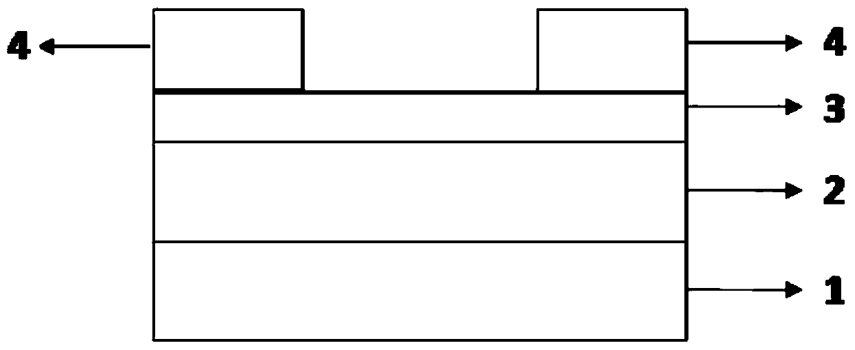
[0042] The gas sensor of the inorganic-organic composite structure heterojunction in this embodiment adopts the top contact form, such as figure 1 As shown, it includes: an inorganic semiconductor layer 2 , an organic semiconductor layer 3 and a metal electrode 4 are sequentially arranged on a substrate 1 .
[0043] The inorganic semiconductor layer 2 is prepared by magnetron sputtering; the organic semiconductor layer 3 is deposited by vacuum thermal evaporation; the metal electrode 4 is prepared by vacuum thermal evaporation deposition, and the metal electrode is located above both ends of the organic semiconductor layer 3 . The appearance of the metal electrodes at both ends of the functional layer adopts the shape of fingers, such as image 3 shown.
[0044] specifically:
[0045]Substrate 1 is a glass substrate;
[0046] The inorganic semiconductor layer 2 is an N-type inorganic semiconductor material with a thickness of 50 nanometers, and the material is indium galliu...
Embodiment 2
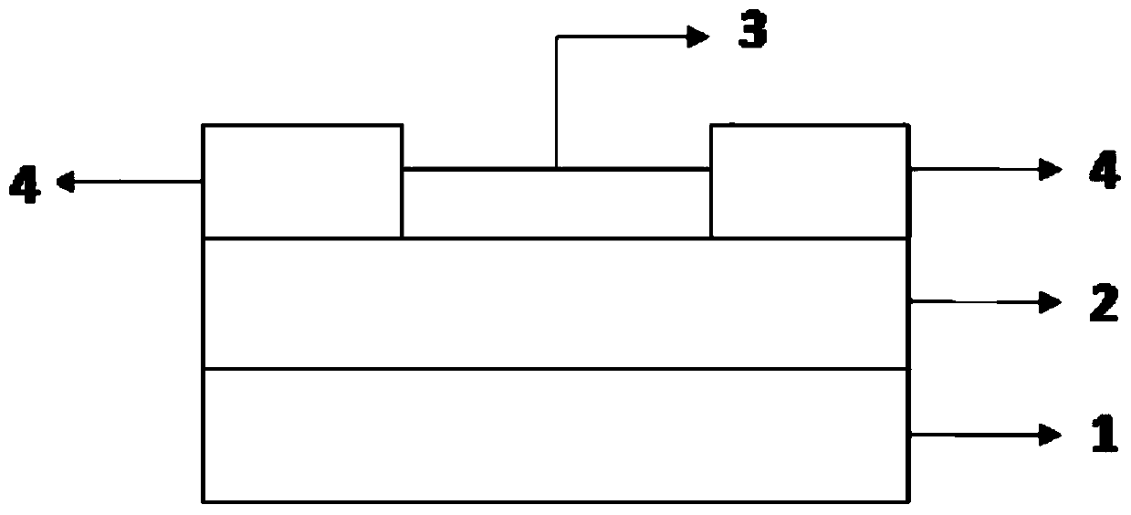
[0050] The gas sensor of the inorganic-organic composite structure heterojunction in this embodiment adopts the bottom contact form, such as figure 2 As shown, it includes: an inorganic semiconductor layer 2 and an organic semiconductor layer 3 are sequentially arranged on the substrate 1. The difference from Embodiment 1 is that the sensor in this embodiment adopts a bottom contact form, and the metal electrode 4 is arranged on the inorganic semiconductor layer. 2, and the metal electrode 4 is located on both sides of the organic semiconductor layer 3, the metal electrode 4 is connected to the organic semiconductor layer 3 and the inorganic semiconductor layer 2, that is, after the inorganic semiconductor layer 2 is prepared, the metal electrode 4 is firstly formed. preparation, followed by the preparation of the organic semiconductor layer 3.
[0051] The inorganic semiconductor layer 2 is prepared by magnetron sputtering; the organic semiconductor layer 3 is prepared by so...
Embodiment 3
[0058] The gas sensor with an inorganic-organic composite structure heterojunction in this embodiment adopts a bottom contact structure, which includes: an inorganic semiconductor layer 2 and an organic semiconductor layer 3 are sequentially arranged on a substrate 1, and the difference from Embodiment 1 lies in: this embodiment The sensor adopts the bottom contact form, the metal electrode 4 is arranged above the two ends of the inorganic semiconductor layer 2, and the metal electrode 4 is located on both sides of the organic metal layer 3, and the metal electrode 4 is connected to both the organic semiconductor layer 3 and the inorganic semiconductor layer 2 , that is, after the inorganic semiconductor layer 2 is prepared, the metal electrode 4 is prepared first, and then the organic semiconductor layer 3 is prepared.
[0059] The inorganic semiconductor layer 2 is prepared by a sol-gel method; the organic semiconductor layer 3 is prepared by a vacuum thermal evaporation meth...
PUM
| Property | Measurement | Unit |
|---|---|---|
| thickness | aaaaa | aaaaa |
| thickness | aaaaa | aaaaa |
| thickness | aaaaa | aaaaa |
Abstract
Description
Claims
Application Information


