HEMT device with back field plate structure and preparation method thereof

A technology of plate structure and back field, which is applied in the field of HEMT devices, can solve the problems of low thermal conductivity of sapphire substrates, achieve the effects of improving electric field distribution, solving back breakdown, and expanding the application range

Pending Publication Date: 2018-01-19
GUANGDONG INST OF SEMICON IND TECH
View PDF16 Cites 3 Cited by
  • Summary
  • Abstract
  • Description
  • Claims
  • Application Information

AI Technical Summary

Problems solved by technology

[0003] In addition, although the sapphire substrate as an insulating material can avoid breakdown at the substrate end, the thermal conductivity of the sapphire substrate is low (~45 W / (m·K)). Under high voltage or high temperature environment, heat dissipation becomes an important issue

Method used


Image

  • HEMT device with back field plate structure and preparation method thereof
  • HEMT device with back field plate structure and preparation method thereof
  • HEMT device with back field plate structure and preparation method thereof

Examples


Embodiment 1

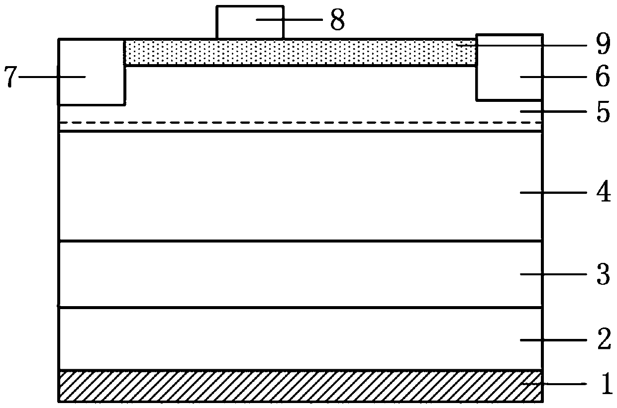
[0027] The structure of the present invention is as figure 1 As shown, from bottom to top are back field plate 1 , substrate 2 , buffer layer 3 , first semiconductor layer 4 , second semiconductor layer 5 and gate oxide layer 9 . Wherein, the drain electrode 6 and the source electrode 7 are provided on the second semiconductor layer 5, the first semiconductor layer 4 and the second semiconductor layer 5 are heterogeneous structures, and a two-dimensional electron gas channel is formed at the interface between the two, The drain 6 and the source 7 form an ohmic contact with the second semiconductor layer 5 and are connected through the two-dimensional electron gas channel. Meanwhile, a gate 8 is provided on the gate oxide layer 9 .

[0028] The materials of each layer in this embodiment are as follows: the back field plate 1 is a single-layer metal material Cu, the substrate 2 is a single-sided polished (0001) sapphire substrate, the buffer layer 3 is an AlN buffer layer, and ...

Embodiment 2

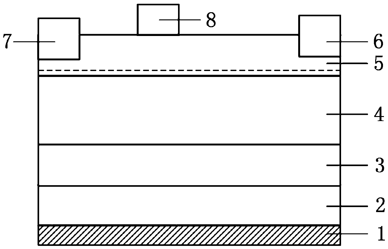
[0038] The structure of the present invention is as figure 2 As shown, from bottom to top are back field plate 1 , substrate 2 , buffer layer 3 , first semiconductor layer 4 and second semiconductor layer 5 . Among them, the drain 6, the source 7 and the gate 8 are arranged on the second semiconductor layer 5, the first semiconductor layer 4 and the second semiconductor layer 5 are heterostructures, and two-dimensional electrons are formed at the interface between the two. The gas channel, the drain 6 and the source 7 form an ohmic contact with the second semiconductor layer 5 and are connected through the two-dimensional electron gas channel.

[0039] The materials of each layer in this embodiment are as follows: the back field plate 1 is a Ni / Au alloy, the substrate 2 is a (001) surface AlN substrate polished on one side, the buffer layer 3 is an AlGaN buffer layer, and the first semiconductor layer 4 is GaN layer, the second semiconductor layer 5 is Al 0.82 In 0.18 The ...


PUM


Abstract

The invention provides an HEMT device with a back field plate structure and a preparation method thereof. The HEMT device comprises a back surface field plate, a substrate, a buffer layer, a first semiconductor layer and a second semiconductor layer which are sequentially arranged from the bottom to the top. The second semiconductor layer is provided with a drain electrode and a source electrode.Both the first semiconductor layer and the second semiconductor layer are heterostructures and a two-dimensional electron gas channel is formed at an interface of the two semiconductor layers, and ohmic contact is formed by the drain and source electrodes and the second semiconductor layer and the drain and source electrodes and the second semiconductor layer are connected through the two-dimensional electron gas channel. When the HEMT device is an MIS structure HEMT device, a surface of the second semiconductor layer between the drain electrode and the source electrode is provided with a gateoxide layer which is provided with a gate. When the HEMT device is an enhanced HEMT device, a surface of the second semiconductor layer between the drain electrode and the source electrode is provided with a gate, and Schottky contact is formed by the gate and the second semiconductor layer. According to the HEMT device and the preparation method thereof, through a high thermal conductivity fieldplate electrode arranged at the back surface of the substrate, the electric field distribution in the device can be improved, the heat dissipation ability of the substrate is enhanced, and thus the voltage withstand characteristic and the high-temperature working performance of the HEMT device are improved.

Description

technical field [0001] The invention relates to a HEMT device, in particular to a back field plate structure HEMT device and a preparation method thereof. Background technique [0002] In order to facilitate compatibility and integration with the current mature silicon process, most current HEMT (High Electron Mobility Transistor, high electron mobility transistor) devices are prepared based on silicon (Si) substrates. However, limited by the huge thermal mismatch and lattice mismatch, gallium nitride (GaN) materials on Si substrates inevitably face problems such as easy cracking and high defect density. Moreover, due to the relatively narrow band gap and poor insulation of Si materials, breakdown from the substrate side is prone to occur when electronic devices work under high field, which greatly limits the application of GaN-based HEMTs under high voltage. . In contrast, the GaN material grown on the sapphire substrate has a relatively small lattice mismatch and thermal...

Claims


Application Information

Patent Timeline
Patent Type & Authority Applications(China)
IPC IPC(8): H01L23/373H01L29/06H01L21/335H01L29/778
Inventor 吴华龙赵维何晨光张康贺龙飞陈志涛
Owner GUANGDONG INST OF SEMICON IND TECH
Why Eureka
Try Eureka